Freescale Semiconductor, Inc.
Parallel Input/Output (I/O)
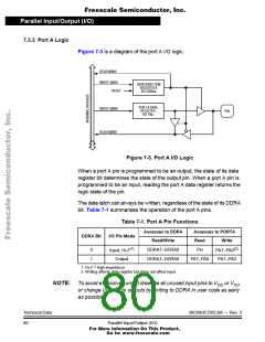
7.3.3 Port A Logic
Figure 7-3 is a diagram of the port A I/O logic.
READ $0004
WRITE $0004
DATA DIRECTION
REGISTER A
RESET
BIT DDRAx
S
U
B
A
T
PORT A DATA
REGISTER
BIT PAx
D
WRITE $0000
L
PAx
READ $0000
Figure 7-3. Port A I/O Logic
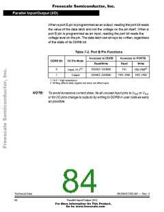
When a port A pin is programmed to be an output, the state of its data
register bit determines the state of the output pin. When a port A pin is
programmed to be an input, reading the port A data register returns the
logic state of the pin.
The data latch can always be written, regardless of the state of its DDRA
bit. Table 7-1 summarizes the operation of the port A pins.
Table 7-1. Port A Pin Functions
Accesses to DDRA
Read/Write
Accesses to PORTA
DDRA Bit
I/O Pin Mode
Read
Pin
Write
(1)
(2)
0
1
DDRA7–DDRA0
DDRA7–DDRA0
Input, Hi-Z
PA7–PA0
Output
PA7–PA0
PA7–PA0
1. Hi-Z = high impedance
2. Writing affects data register but does not affect input.
NOTE: To avoid excessive current draw, tie all unused input pins to VDD or VSS,
or change I/O pins to outputs by writing to DDRA in user code as early
as possible.
Technical Data
80
MC68HC705C8A — Rev. 3
Parallel Input/Output (I/O)
For More Information On This Product,
Go to: www.freescale.com

 FREESCALE [ Freescale ]