Freescale Semiconductor, Inc.
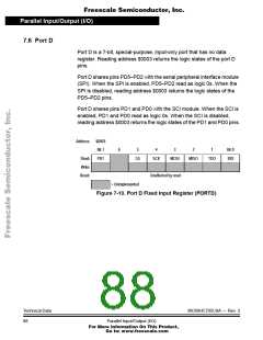
Parallel Input/Output (I/O)
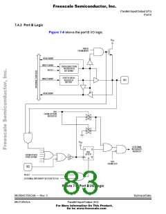
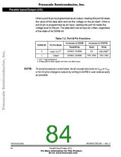
When a port B pin is programmed as an output, reading the port bit reads
the value of the data latch and not the voltage on the pin itself. When a
port B pin is programmed as an input, reading the port bit reads the
voltage level on the pin. The data latch can always be written, regardless
of the state of its DDRB bit.
Table 7-2. Port B Pin Functions
Accesses to DDRB
Read/Write
Accesses to PORTB
DDRB Bit
I/O Pin Mode
Read
Pin
Write
(1)
(2)
0
1
DDRB7–DDRB0
DDRB7–DDRB0
Input, Hi-Z
PB7–PB0
Output
PB7–PB0
PB7–PB0
1. Hi-Z = high impedance
2. Writing affects data register but does not affect input.
NOTE: To avoid excessive current draw, tie all unused input pins to VDD or VSS,
or for I/O pins change to outputs by writing to DDRB in user code as early
as possible.
Technical Data
84
MC68HC705C8A — Rev. 3
Parallel Input/Output (I/O)
For More Information On This Product,
Go to: www.freescale.com

 FREESCALE [ Freescale ]