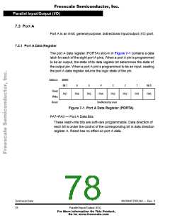
Freescale Semiconductor, Inc.
Parallel Input/Output (I/O)
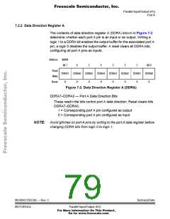
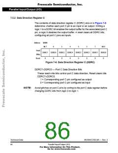
7.4.2 Data Direction Register B
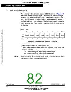
The contents of data direction register B (DDRB) shown in Figure 7-5
determine whether each port B pin is an input or an output. Writing a
logic 1 to a DDRB bit enables the output buffer for the associated port B
pin; a logic 0 disables the output buffer. A reset clears all DDRB bits,
configuring all port B pins as inputs. If the pullup devices are enabled by
mask option, setting a DDRB bit to a logic 1 turns off the pullup device
for that pin.
Address: $0005
Bit 7
DDRB7
0
6
DDRB6
0
5
DDRB5
0
4
DDRB4
0
3
DDRB3
0
2
DDRB2
0
1
DDRB1
0
Bit 0
DDRB0
0
Read:
Write:
Reset:
Figure 7-5. Data Direction Register B (DDRB)
DDRB7–DDRB0 — Port B Data Direction Bits
These read/write bits control port B data direction. Reset clears bits
DDRB7–DDRB0.
1 = Corresponding port B pin configured as output
0 = Corresponding port B pin configured as input
NOTE: Avoid glitches on port B pins by writing to the port B data register before
changing DDRB bits from logic 0 to logic 1.
Technical Data
82
MC68HC705C8A — Rev. 3
Parallel Input/Output (I/O)
For More Information On This Product,
Go to: www.freescale.com

 FREESCALE [ Freescale ]