Freescale Semiconductor, Inc.
MC68HSC705C8A
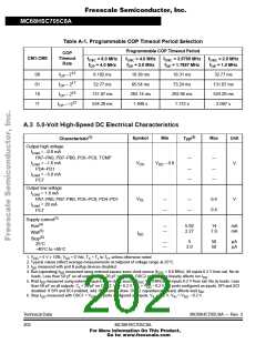
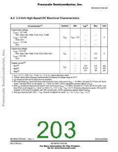
A.4 3.3-Volt High-Speed DC Electrical Characteristics
(1)
(2)
Symbol
Min
Max
Unit
Characteristic
Output high voltage
Typ
I
I
I
= –0.2 mA
Load
PA7–PA0, PB7–PB0, PC6–PC0, TCMP
= –0.4 mA
—
—
—
—
—
—
V
V
– 0.3
DD
V
Load
OH
PD4–PD1
= –1.5 mA
Load
PC7
Output low voltage
I
I
= 0.4 mA
Load
V
PA7–PA0, PB7–PB0, PC6–PC0, PD4–PD1
= 6.0 mA
—
—
—
—
0.3
0.3
V
OL
Load
PC7
(3)
Supply current
(4)
Run
—
—
—
1.91
0.915
2.0
6.0
2.0
20
mA
mA
µA
I
DD
(5)
Wait
(6)
Stop
1. V = 3.3 V ± 10%; V = 0 Vdc, T = T to T , unless otherwise noted
DD
SS
A
L
H
2. Typical values reflect average measurements at midpoint of voltage range at 25°C.
3. I measured with port B pullup devices disabled.
DD
4. Run (operating) I measured using external square wave clock source (f
= 4.2 MHz). All inputs 0.2 V from rail. No dc
DD
OSC
loads. Less than 50 pF on all outputs. C = 20 pF on OSC2. OSC2 capacitance linearly affects run I
.
DD
L
5. Wait I measured using external square wave clock source (f
= 4.2 MHz). All inputs 0.2 V from rail. No dc loads. Less
DD
OSC
than 50 pF on all outputs. C = 20 pF on OSC2. V = 0.2 V, V = V – 0.2 V. All ports configured as inputs. SPI and SCI
L
IL
IH
DD
disabled. If SPI and SCI enabled, add 10% current draw. OSC2 capacitance linearly affects wait IDD
.
6. Stop I measured with OSC1 = V . All ports configured as inputs. V = 0.2 V; V = V – 0.2 V.
DD
DD
IL
IH
DD
MC68HC705C8A — Rev. 3
MOTOROLA
Technical Data
MC68HSC705C8A
For More Information On This Product,
Go to: www.freescale.com

 FREESCALE [ Freescale ]