Freescale Semiconductor, Inc.
MC68HSC705C8A
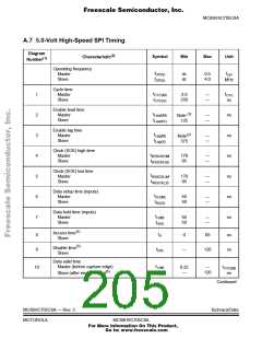
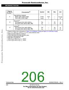
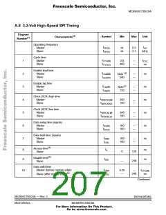
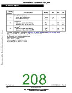
Diagram
(2)
Symbol
Min
Max
Unit
Characteristic
(1)
Number
Data hold time (outputs)
t
t
11
12
13
Master (after capture edge)
Slave (after enable edge)
0.25
0
—
—
HO(M)
CYC(M)
t
ns
HO(S)
(7)
Rise time
t
—
—
50
2.0
ns
µs
RM
SPI outputs (SCK, MOSI, MISO)
SPI inputs (SCK, MOSI, MISO, SS)
t
RS
(8)
Fall time
t
—
—
50
2.0
ns
µs
FM
SPI outputs (SCK, MOSI, MISO)
SPI inputs (SCK, MOSI, MISO, SS)
t
FS
1. Diagram numbers refer to dimensions in Figure 13-8. SPI Master Timing and Figure 13-9. SPI Slave Timing.
2. V = 5 V ± 10%; V = 0 Vdc, T = T to T , unless otherwise noted
DD
SS
A
L
H
3. Signal production depends on software.
4. Time to data active from high-impedance state
5. Hold time to high-impedance state
6. With 200 pF on all SPI pins.
7. 20% of V to 70% of V ; C = 200 pF
DD
DD
L
8. 70% of V to 20% of V ; C = 200 pF
DD
DD
L
Technical Data
206
MC68HC705C8A — Rev. 3
MC68HSC705C8A
For More Information On This Product,
Go to: www.freescale.com

 FREESCALE [ Freescale ]