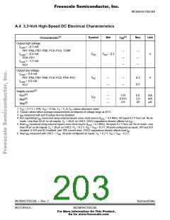
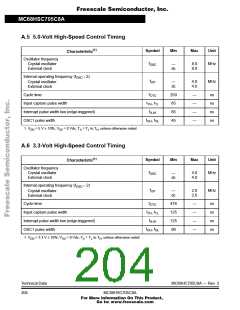
Freescale Semiconductor, Inc.
MC68HSC705C8A
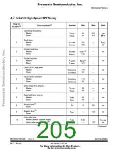
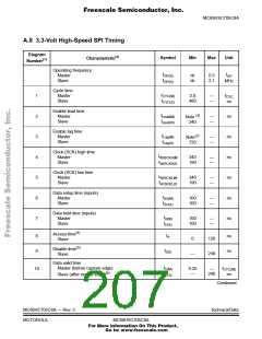
A.8 3.3-Volt High-Speed SPI Timing
Diagram
(2)
Symbol
Min
Max
Unit
Characteristic
Operating frequency
(1)
Number
f
f
Master
Slave
dc
dc
0.5
2.1
OP(S)
OP
f
MHz
OP(S)
Cycle time
Master
t
t
1
2
3
4
5
6
7
2.0
480
—
—
CYC(M)
CYC
Slave
t
ns
CYC(S)
Enable lead time
Master
(3)
t
—
—
ns
Lead(M)
Note
240
Slave
t
Lead(S)
Enable lag time
Master
(2)
t
—
—
ns
ns
ns
ns
ns
Lag(M)
Note
720
Slave
t
Lag(S)
Clock (SCK) high time
Master
t
340
190
—
—
W(SCKH)M
Slave
t
W(SCKH)S
Clock (SCK) low time
Master
t
340
190
—
—
W(SCKL)M
Slave
t
W(SCKL)S
Data setup time (inputs)
t
Master
Slave
100
100
—
—
SU(M)
t
SU(S)
Data hold time (inputs)
t
Master
Slave
100
100
—
—
H(M)
t
H(S)
(4)
Access time
t
8
9
ns
ns
A
0
120
240
Slave
(5)
Disable time
t
DIS
—
Slave
Data valid time
t
Master (before capture edge)
t
10
0.25
—
—
240
V(M)
CYC(M)
(6)
t
ns
Slave (after enable edge)
V(S)
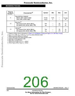
Continued
MC68HC705C8A — Rev. 3
MOTOROLA
Technical Data
MC68HSC705C8A
For More Information On This Product,
Go to: www.freescale.com

 FREESCALE [ Freescale ]