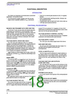
ELECTRICAL CHARACTERISTICS
DYNAMIC ELECTRICAL CHARACTERISTICS
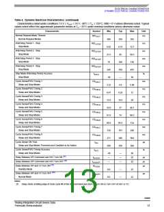
Table 4. Dynamic Electrical Characteristics (continued)
Characteristics noted under conditions 7.0 V ≤ VSUP ≤ 18 V, -40°C ≤ TA ≤ 125°C, GND = 0 V unless otherwise noted. Typical
values noted reflect the approximate parameter means at TA = 25°C under nominal conditions unless otherwise noted.
Characteristic
Symbol
Min
Typ
Max
Unit
Delay Between Normal Request and Normal Mode After WD Trigger Command
Normal Request Mode
tS
µs
NR2N
15
—
35
—
70
10
Delay Between SPI and CAN Normal Mode
SBC Normal Mode (26)
tS
µs
µs
µs
CANN
Delay Between SPI and CAN Normal Mode
SBC Normal Mode (26)
tS
CANS
—
—
10
Delay Between CS Wake-up (CS Low to High) and SBC Normal Request Mode
tWCS
(V
on and Reset High)
DD1
SBC in Stop Mode
15
40
90
Delay Between CS Wake-up (CS Low to High) and First Accepted API
Command
tW
µs
µs
SPI
90
20
—
—
N/A
SBC in Stop Mode
Delay Between INT Pulse and First SPI Command Accepted
In Stop Mode After Wake-up
tS
1STSPI
N/A
38
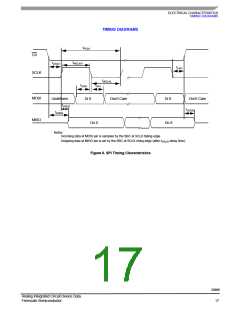
INPUT TERMINNALS (L0, L1, L2, AND L3)
Wake-up Filter Time
t
8.0
20
µs
WUF
CAN MODULE-SIGNAL EDGE RISE AND FALL TIMES (CANH, CANL)
Dominant State Timeout
t
200
360
520
µs
ns
DOUT
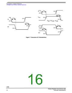
Propagation Loop Delay TX to RX, Recessive to Dominant
t
LRD
TRD
RRD
Slew Rate 3
Slew Rate 2
Slew Rate 1
Slew Rate 0
70
80
140
155
180
220
210
225
255
310
100
110
Propagation Delay TX to CAN
Slew Rate 3
t
ns
20
40
65
80
110
150
200
300
Slew Rate 2
Slew Rate 1
60
120
160
Slew Rate 0
100
Propagation Delay CAN to RX, Recessive to Dominant
t
30
80
140
ns
ns
Propagation Loop Delay TX to RX, Dominant to Recessive
t
LDR
TDR
RDR
Slew Rate 3
Slew Rate 2
Slew Rate 1
Slew Rate 0
70
90
120
135
160
200
170
180
220
260
100
130
Propagation Delay TX to CAN
Slew Rate 3
t
ns
60
65
75
90
110
120
150
190
130
150
200
300
Slew Rate 2
Slew Rate 1
Slew Rate 0
Propagation Delay CAN to RX, Dominant to Recessive
t
20
40
60
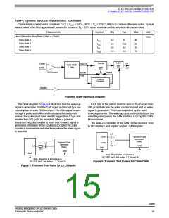
Notes
26. Guaranteed by design; however, it is not production tested.
33989
Analog Integrated Circuit Device Data
Freescale Semiconductor
14

 FREESCALE [ Freescale ]