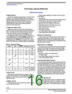
FUNCTIONAL DEVICE OPERATION
OPERATIONAL MODES
FUNCTIONAL DEVICE OPERATION
OPERATIONAL MODES
Control register settings from a Power-ON Reset (POR)
are as follows:
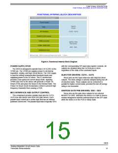
POWER SUPPLY
The 33810 is designed to operate from 4.5V to 36V on the
VPWR pin. The VPWR pin supplies power to all internal
regulators, analog and logic circuit blocks. The VDD supply is
used for setting communication threshold levels and
supplying power to the SO driver. This IC architecture
provides flexible microprocessor interfacing and low
quiescent current sleep mode.
• All outputs off
• IGNITION gate driver mode enabled (IGBT Ignition Mode).
• PWM frequency and duty cycle control disabled.
• Off State open load detection enabled (LSD)
• MAXI dac set to 14A, NOMI DAC set to 5.5A
• Spark detect level VIL DAC set to VPWR +5.5V
• Open secondary timer set to 100µs
• Dwell timer set 32ms
POWER-ON RESET (POR)
Applying VPWR and VDD to the device will generate a
Power On Reset (POR) and place the device in the Normal
State. The Power On Reset circuit incorporates a filter to
prevent high frequency transients from causing a POR.
• Soft shutdown disabled
• Low-voltage flyback clamp disabled
• Dwell overlap MAXI offset disabled
All outputs are disabled when the OUTEN input pin is
HIGH regardless of the SPI control registers or the logic level
on the parallel input pins. With the OUTEN pin high, SPI
messages may be sent and received by the device. Upon
enabling the device (OUTEN low), outputs will be activated
based on the state of the command register or parallel input.
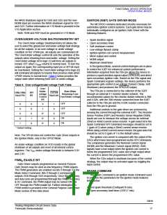
MODES OF OPERATION
In Normal State, the 33810 gate driver has three modes of
operation, ignition Mode, GPGD (General Purpose Gate
Driver) Mode and V10 mode.The operating mode of each
gate driver may be set individually and is programmed using
the Mode Select Command.
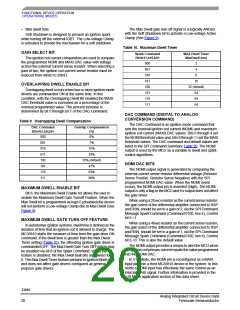
Table 5. Operational States
MODE SELECT COMMAND
VPWR
VDD
OUTEN
OUTPUTS
STATE
The MODE Select Command is used to set the operating
mode for the GDx gate driver outputs, over/under-voltage
operation and to enable V10 Mode and the PWM generators.
The Mode Select Command programmable features are
listed below.
L
L
X
OFF
Power
Off
L
H
H
H
L
X
X
X
OFF
OFF
OFF
POR
SLEEP
POR
• Ignition/GPGD Mode select (gate drivers)
• V10 Mode enable
• Over/Under-voltage operation for all drivers
• GPGD PWM controller enable
H
L
X
X
OFF
OFF
POR
IGNITION/GPGD MODE SELECT
The Ignition/General Purpose Gate Driver Mode select bits
determine independently, the operating mode of each of the
GDx gate driver outputs. Bits 8,9,10,11 correspond to GD0,
GD1, GD2, GD3 respectively. Setting the bit to a logic 0 sets
the GDx driver to the Ignition Mode. Setting the bit to a logic
1 commands the GDX driver to the General Purpose Mode
and disables the ignition features for that particular gate
driver (except the MAXI current shutdown feature). Further
information on GDx gate driver in Ignition Mode and General
Purpose Mode is provided later in this section of the data
sheet.
SLEEP
H
H
H
H
L
ACTIVE
OFF
NORMAL
NORMAL
H
SLEEP STATE
Sleep State is entered when the VDD supply voltage is
removed from the VDD pin. In Sleep State all outputs are off.
Applying VDD will force the device to exit the Sleep State and
generates a POR.
V10 MODE ENABLE BIT
The V10 Enable bit allows the user to configure the device
for 10 cylinder applications. When the V10 Mode is enabled,
the device configures the NOMI pin and MAXI pin as digital
inputs rather than outputs. The new MAXI input pin receives
NORMAL STATE
The default Normal State is entered when power is applied
to the VPWR and VDD pins.
33810
Analog Integrated Circuit Device Data
Freescale Semiconductor
16

 FREESCALE [ Freescale ]