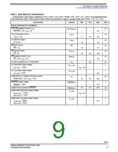
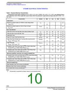
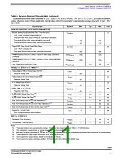
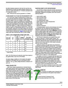
FUNCTIONAL DESCRIPTION
FUNCTIONAL PIN DESCRIPTION
FUNCTIONAL DESCRIPTION
FUNCTIONAL PIN DESCRIPTION
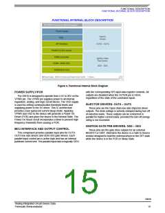
ANALOG SUPPLY VOLTAGE (VPWR)
SERIAL INPUT DATA (SI)
The VPWR pin is the battery input to the 33810 IC. The
VPWR pin requires external reverse battery and transient
protection. All IC analog current and internal logic current is
provided from the VPWR pin. With VDD applied to the IC, the
application of VPWR will perform a POR.
The SI pin is used for serial instruction data input. SI
information is latched into the input register on the rising edge
of SCLK. A logic high state present on SI will program a one
in the command word on the rising edge of the CS signal. To
program a complete word, 16 bits of information or multiples
of 8 there of must be entered into the device.
DIGITAL LOGIC SUPPLY VOLTAGE (VDD)
SERIAL OUTPUT DATA (SO)
The VDD input pin is used to determine communication
logic levels between the microprocessor and the 33810 IC.
Current from VDD is used to drive SO output and the pull-up
current for CS. VDD must be applied for normal mode
operation. Removing VDD from the IC will place the device in
sleep mode. With VPWR applied to the IC, the application of
VDD will perform a POR.
The SO pin is the output from the shift register. The SO pin
remains tri-stated until the CS pin transitions to a logic low
state. All normal operating drivers are reported as zero, all
faulted drivers are reported as one. The negative transition of
CS enables the SO driver.
The SI/SO shifting of the data follows a first-in-first-out
protocol, with both input and output words transferring the
most significant bit (MSB) first.
GROUND (GND)
The bottom pad or FLAG provides the only ground
connection for the IC. The VPWR and VDD supplies are both
referenced to the GND pad. The GND pad is used for both
de-coupling the power supplies as well as power ground for
the output drivers. Although the silicon die is epoxy attached
to the top side of the pad, the pad must be grounded for
proper electrical operation.
OUTPUT ENABLE (OUTEN)
The OUTEN pin is an active low input. When the OUTEN
pin is low, all the device outputs are active. The outputs are
all disabled when OUTEN pin is high. SPI and parallel
communications are still active in either state of OUTEN.
FEEDBACK VOLTAGE SENSOR (FB0-FB3)
SERIAL CLOCK INPUT (SCLK)
The FBx pin has multiple functions for control and
diagnostics of the external MOSFET/IGBT Ignition gate
driver.
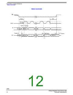
The system clock (SCLK) pin clocks the internal shift
register of the 33810. The SI data is latched into the input
shift register on the rising edge of SCLK signal. The SO pin
shifts status bits out on the falling edge of SCLK. The SO data
is available for the MCU to read on the rising edge of SCLK.
With CS in a logic high state, signals on the SCLK and SI pins
will be ignored and the SO pin is tri-state
In Ignition (IGBT) Gate Driver Mode, the feedback inputs
monitor the IGBT's collector voltage to provide the spark
duration timer control signal. The spark duration timer
monitors this input to determine if the secondary clamp
function should be activated. In secondary clamp mode, the
IGBT's collector voltage is internally clamped to VPWR+11V.
CHIP SELECT (CS)
In the General Purpose Gate Driver mode, this input
monitors the drain of an external MOSFET to provide short-
circuit and open circuit detection by monitoring the
MOSFET's drain to source voltage. The filter timer and
threshold voltage are easily programmed through SPI (See
tables 18 and 19 for SPI messages).
The system MCU selects the 33810 to receive
communication using the chip select (CS) pin. With the CS in
a logic low state, command words may be sent to the 33810
via the serial input (SI) pin, and status information is received
by the MCU via the serial output (SO) pin. The falling edge of
CS enables the SO output and transfers status information
into the SO buffer.
In General Purpose Gate Driver mode the FBx pin also
provides a drain to gate clamp for fast turn off of inductive
loads and external MOSFET protection.
Rising edge of the CS initiates the following operation:
Disables the SO driver (high-impedance)
GATE DRIVER OUTPUT (GD0-GD3)
Activates the received command word, allowing the 33810
to activate/deactivate output drivers.
The GDX pins are the gate drive outputs for an external
MOSFET or IGBT. Internal to the device is a Gate to Source
resistor designed to hold the external device in the OFF state
while the device is in the POR or SLEEP state.
To avoid any spurious data, it is essential that the high-to-
low and low-to-high transitions of the CS signal occur only
when SCLK is in a logic low state. Internal to the 33810
device is an active pull-up to VDD on CS.
33810
Analog Integrated Circuit Device Data
Freescale Semiconductor
13

 FREESCALE [ Freescale ]