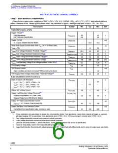
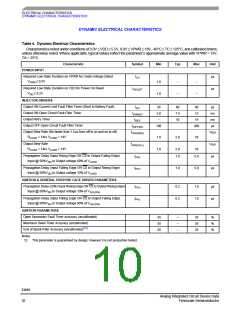
ELECTRICAL CHARACTERISTICS
DYNAMIC ELECTRICAL CHARACTERISTICS
DYNAMIC ELECTRICAL CHARACTERISTICS
Table 4. Dynamic Electrical Characteristics
Characteristics noted under conditions of 3.0V ≤ VDD ≤ 5.5V, 9.0V ≤ VPWR ≤ 18V, -40°C ≤ TC ≤ 125°C, and calibrated timers,
unless otherwise noted. Where applicable, typical values reflect the parameter’s approximate average value with VPWR = 13V,
TA = 25°C.
Characteristic
Symbol
Min
Typ
Max
Unit
POWER INPUT
Required Low State Duration on VPWR for Under-voltage Detect
tUV
µs
µs
VPWR ≤ 0.2V
1.0
1.0
–
–
–
–
Required Low State Duration on VDD for Power On Reset
t
RESET
VDD ≤ 0.2V
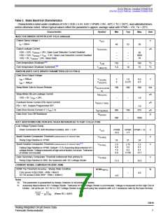
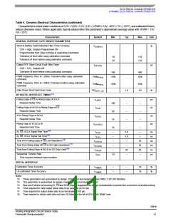
INJECTOR DRIVERS
Output ON Current Limit Fault Filter Timer (Short to Battery Fault)
Output ON Open Circuit Fault Filter Timer
Output Retry Timer
t
30
3.0
–
60
7.5
10
90
12
µs
ms
ms
µs
SC
t(ON)OC
t
15
REF
Output OFF Open Circuit Fault Filter Timer
Output Slew Rate (No faster than 1.5µs from off to on and on to off)
t(OFF)OC
100
400
tSR(RISE)
V/µs
R
= 14Ω, VLOAD = 14V
1.0
1.0
5.0
10
LOAD
Output Slew Rate
= 14Ω, VLOAD = 14V
tSR(FALL)
V/µs
µs
R
5.0
1.0
10
LOAD
Propagation Delay (Input Rising Edge OR CS to Output Falling Edge)
Input @ 50%VDD to Output voltage 90% of VLOAD
tPHL
5.0
Propagation Delay (Input Falling Edge OR CS to Output Rising Edge)
Input @ 50%VDD to Output voltage 10% of VLOAD
tPLH
1.0
5.0
µs
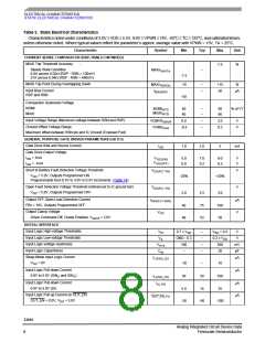
IGNITION & GENERAL PURPOSE GATE DRIVER PARAMETERS
Propagation Delay (GINx Input Rising Edge OR CS to Output Rising Edge)
tPLH
0.2
0.2
1.0
1.0
µs
µs
Input @ 50%VDD to Output voltage 10% of V
GS(ON)
Propagation Delay (Input Falling Edge OR CS to Output Falling Edge)
tPHL
Input @ 50%VDD to Output voltage 90% of V
GS(ON)
IGNITION PARAMETERS
Open Secondary Fault Timer accuracy (uncalibrated)
Maximum Dwell Timer Accuracy (uncalibrated)
End of Spark Filter Accuracy (uncalibrated)(12)
Notes
-35
-35
-35
–
–
–
35
35
35
%
%
%
12. This parameter is guaranteed by design, however it is not production tested.
33810
Analog Integrated Circuit Device Data
Freescale Semiconductor
10

 FREESCALE [ Freescale ]