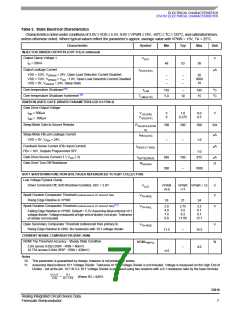
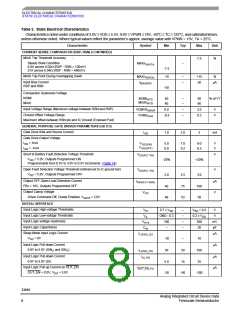
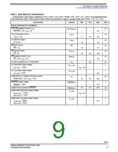
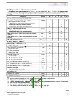
ELECTRICAL CHARACTERISTICS
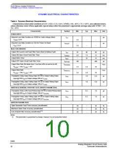
DYNAMIC ELECTRICAL CHARACTERISTICS
Table 4. Dynamic Electrical Characteristics (continued)
Characteristics noted under conditions of 3.0V ≤ VDD ≤ 5.5V, 9.0V ≤ VPWR ≤ 18V, -40°C ≤ TC ≤ 125°C, and calibrated timers,
unless otherwise noted. Where applicable, typical values reflect the parameter’s approximate average value with VPWR = 13V,
TA = 25°C.
Characteristic
Symbol
Min
Typ
Max
Unit
GENERAL PURPOSE GATE DRIVER PARAMETERS
Short to Battery Fault Detection Filter Timer Accuracy
VDD = High, Outputs Programmed ON
V
%
DS(flt-th)
Programmable from 30µs to 960µs in replicating increments
Tolerance of timer after using calibration command
Tolerance of timer before using calibration command
-10
-35
+10
+35
Output OFF Open Circuit Fault Filter Timer
VDD = 5.0V, Outputs Off
t(OFF)OC
µs
Tolerance of timer before using calibration command
100
400
PWM Frequency 10Hz to 1.28kHz Tolerance after using calibration
command
PWM
PWM
-10%
10%
FREQ
PWM Frequency 10Hz to 1.28kHz Tolerance before using calibration
command
-35%
35%
3.0
FREQ
Gate Driver Short Fault Duty Cycle
GD
1.0
%
SHRT_DC
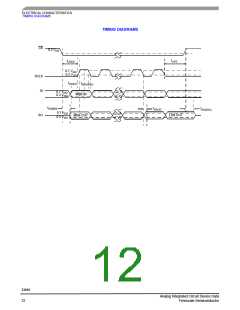
SPI DIGITAL INTERFACE TIMING(13)
Falling Edge of CS to Rising Edge of SCLK
Required Setup Time
t
ns
ns
ns
ns
LEAD
100
50
–
–
–
–
–
–
Falling Edge of SCLK to Rising Edge of CS
Required Setup Time
t
LAG
SI(SU)
SI to Rising Edge of SCLK
Required Setup Time
t
16
Rising Edge of SCLK to SI
Required Hold Time
t
SI(HOLD)
20
–
–
5.0
5.0
–
–
–
SI, CS, SCLK Signal Rise Time(14)
t
t
ns
ns
ns
ns
ns
µs
R(SI)
F(SI)
SI, CS, SCLK Signal Fall Time(15)
–
–
Time from Falling Edge of CS Low-impedance(16)
Time from Rising Edge off CS to SO High-impedance(17)
Time from Falling Edge of SCLK to SO Data Valid(18)
t
–
55
55
55
–
SO(EN)
t
–
–
SO(DIS)
t
–
25
–
VALID
tSTR
Sequential Transfer Rate
1.0
Time required between data transfers
DIGITAL INTERFACE
Calibrated Timer Accuracy
Un-calibrated Timer Accuracy
Notes
t
–
–
–
–
10
35
%
%
TIMER
TIMER
t
13. These parameters are guaranteed by design. Production test equipment uses 1MHz, 5.0V SPI interface.
14. This parameter is guaranteed by design, however it is not production tested.
15. Rise and Fall time of incoming SI, CS and SCLK signals suggested for design consideration to prevent the occurrence of double pulsing.
16. Time required for valid output status data to be available on SO pin.
17. Time required for output states data to be terminated at SO pin.
18. Time required to obtain valid data out from SO following the fall of SCLK with 200pF load.
33810
Analog Integrated Circuit Device Data
Freescale Semiconductor
11

 FREESCALE [ Freescale ]