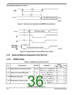
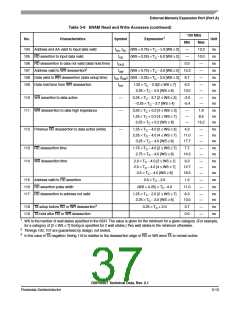
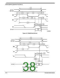
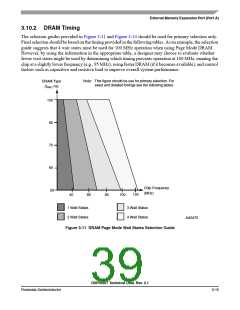
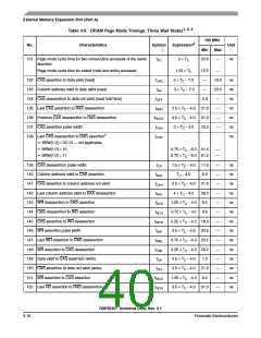
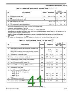
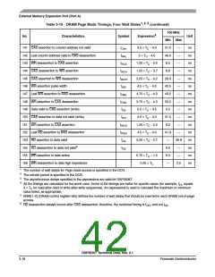
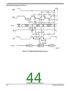
External Memory Expansion Port (Port A)
Table 3-9 DRAM Page Mode Timings, Three Wait States1, 2, 3
100 MHz
No.
Characteristics
Symbol
Expression4
Unit
Min
Max
131 Page mode cycle time for two consecutive accesses of the same
direction
tPC
2 × TC
20.0
—
ns
Page mode cycle time for mixed (read and write) accesses
1.25 × TC
2 × TC − 7.0
3 × TC − 7.0
12.5
—
—
13.0
23.0
—
132 CAS assertion to data valid (read)
tCAC
tAA
ns
ns
ns
ns
ns
ns
ns
133 Column address valid to data valid (read)
134 CAS deassertion to data not valid (read hold time)
135 Last CAS assertion to RAS deassertion
136 Previous CAS deassertion to RAS deassertion
137 CAS assertion pulse width
—
tOFF
tRSH
tRHCP
tCAS
tCRP
0.0
2.5 × TC − 4.0 21.0
4.5 × TC − 4.0 41.0
—
—
2 × TC − 4.0
16.0
—
138 Last CAS deassertion to RAS assertion5
• BRW[1:0] = 00, 01— not applicable
• BRW[1:0] = 10
4.75 × TC − 6.0 41.5
6.75 × TC − 6.0 61.5
—
—
• BRW[1:0] = 11
139 CAS deassertion pulse width
tCP
tASC
tCAH
tRAL
tRCS
tRCH
tWCH
tWP
1.5 × TC − 4.0 11.0
—
—
—
—
—
—
—
—
—
—
—
—
—
—
ns
ns
ns
ns
ns
ns
ns
ns
ns
ns
ns
ns
ns
ns
140 Column address valid to CAS assertion
141 CAS assertion to column address not valid
142 Last column address valid to RAS deassertion
143 WR deassertion to CAS assertion
144 CAS deassertion to WR assertion
145 CAS assertion to WR deassertion
146 WR assertion pulse width
TC − 4.0
2.5 × TC − 4.0 21.0
4 × TC − 4.0 36.0
1.25 × TC − 4.0 8.5
0.75 × TC − 4.0 3.5
6.0
2.25 × TC − 4.2 18.3
3.5 × TC − 4.5 30.5
3.75 × TC − 4.3 33.2
3.25 × TC − 4.3 28.2
147 Last WR assertion to RAS deassertion
148 WR assertion to CAS deassertion
149 Data valid to CAS assertion (write)
150 CAS assertion to data not valid (write)
151 WR assertion to CAS assertion
tRWL
tCWL
tDS
0.5 × TC − 4.0
1.0
tDH
2.5 × TC − 4.0 21.0
1.25 × TC − 4.3 8.2
3.5 × TC − 4.0 31.0
tWCS
tROH
152 Last RD assertion to RAS deassertion
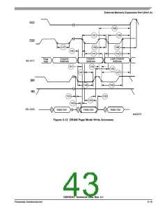
DSP56367 Technical Data, Rev. 2.1
3-16
Freescale Semiconductor

 FREESCALE [ Freescale ]