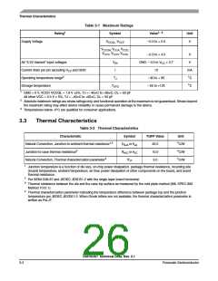
Thermal Characteristics
Table 3-1 Maximum Ratings
Symbol
Rating1
Value1, 2
Unit
Supply Voltage
VCCQL, VCCP
−0.3 to + 2.0
V
VCCQH, VCCA, VCCD,
VCCC, VCCH, VCCS,
−0.3 to + 4.0
GND − 0.3 to VCC + 0.7
10
V
V
All “3.3V tolerant” input voltages
Current drain per pin excluding VCC and GND
Operating temperature range3
Storage temperature
VIN
I
mA
°C
°C
TJ
−40 to + 95
TSTG
−55 to +125
1
2
3
GND = 0 V, VCCP, VCCQL = 1.8 V 5%, TJ = –40×C to +95×C, CL = 50 pF
All other VCC = 3.3 V 5%, TJ = –40×C to +95×C, CL = 50 pF
Absolute maximum ratings are stress ratings only, and functional operation at the maximum is not guaranteed. Stress beyond
the maximum rating may affect device reliability or cause permanent damage to the device.
Temperatures below -0°C are qualified for consumer applications.
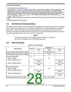
3.3
Thermal Characteristics
Table 3-2 Thermal Characteristics
Characteristic
Symbol
RθJA or θJA
RθJC or θJC
ΨJT
TQFP Value
45.0
Unit
°C/W
°C/W
°C/W
Natural Convection, Junction-to-ambient thermal resistance1,2
Junction-to-case thermal resistance3
10.0
Natural Convection, Thermal characterization parameter4
3.0
1
Junction temperature is a function of die size, on-chip power dissipation, package thermal resistance, mounting site
(board) temperature, ambient temperature, air flow, power dissipation of other components on the board, and board
thermal resistance.
2
3
Per SEMI G38-87 and JEDEC JESD51-2 with the single layer board horizontal.
Thermal resistance between the die and the case top surface as measured by the cold plate method (MIL SPEC-883
Method 1012.1).
4
Thermal characterization parameter indicating the temperature difference between package top and the junction
temperature per JEDEC JESD51-2. When Greek letters are not available, the thermal characterization parameter is
written as Psi-JT.
DSP56367 Technical Data, Rev. 2.1
3-2
Freescale Semiconductor

 FREESCALE [ Freescale ]