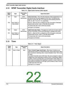
JTAG/OnCE Interface
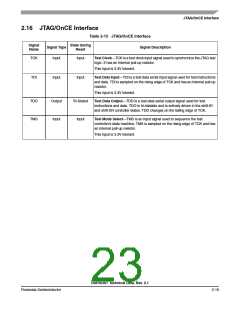
2.16 JTAG/OnCE Interface
Table 2-15 JTAG/OnCE Interface
Signal
Name
State during
Signal Type
Signal Description
Reset
TCK
Input
Input
Test Clock—TCK is a test clock input signal used to synchronize the JTAG test
logic. It has an internal pull-up resistor.
This input is 3.3V tolerant.
TDI
Input
Input
Test Data Input—TDI is a test data serial input signal used for test instructions
and data. TDI is sampled on the rising edge of TCK and has an internal pull-up
resistor.
This input is 3.3V tolerant.
TDO
TMS
Output
Input
Tri-Stated
Input
Test Data Output—TDO is a test data serial output signal used for test
instructions and data. TDO is tri-statable and is actively driven in the shift-IR
and shift-DR controller states. TDO changes on the falling edge of TCK.
Test Mode Select—TMS is an input signal used to sequence the test
controller’s state machine. TMS is sampled on the rising edge of TCK and has
an internal pull-up resistor.
This input is 3.3V tolerant.
DSP56367 Technical Data, Rev. 2.1
Freescale Semiconductor
2-19

 FREESCALE [ Freescale ]