Freescale Semiconductor, Inc.
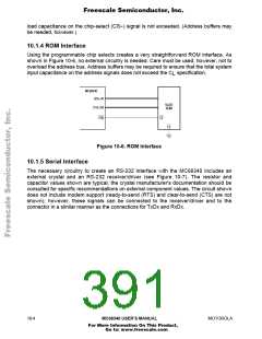
15 pF
X1
3.6864 MHz
X2
5 pF
MC68340
Rx1
RxDx
TxDx
R
Tx1
T
MC145407
V
CC
C1+ C2+
µ
10 µF
10 µ F
10
F
C1-
C1-
VSS
C2+
C2-
10 µ F
GND
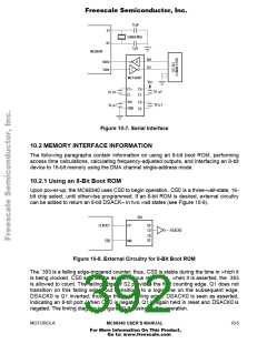
Figure 10-7. Serial Interface
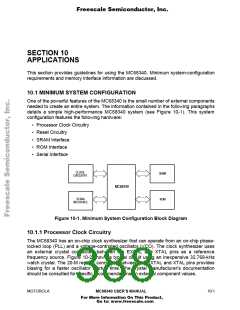
10.2 MEMORY INTERFACE INFORMATION
The following paragraphs contain information on using an 8-bit boot ROM, performing
access time calculations, calculating frequency-adjusted outputs, and interfacing an 8-bit
device to 16-bit memory using the DMA channel single-address mode.
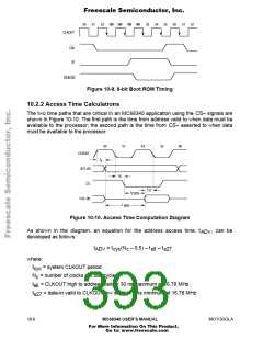
10.2.1 Using an 8-Bit Boot ROM
Upon power-up, the MC68340 uses CS0 to begin operation. CS0 is a three-wait-state, 16-
bit chip select, until otherwise programmed. If an 8-bit ROM is desired, external circuitry
can be added to return an 8-bit DSACK≈ in two wait states (see Figure 10-8).
'393
CLKOUT
CS0
CP
Q0
Q1
Q2
Q3
DSACK0
MR
Figure 10-8. External Circuitry for 8-Bit Boot ROM
The `393 is a falling edge-triggered counter; thus, CS0 is stable during the time in which it
is being clocked. CS0 acts as the asynchronous reset—i.e., when it is asserted, the `393
is allowed to count. The falling edge of S2 provides the first counting edge. Q1 does not
transition on this falling edge, but transitions to a logic one on the subsequent edge.
DSACK0 is Q1 inverted; thus, on the next falling edge, DSACK0 is seen as asserted,
indicating an 8-bit port. When CS0 is negated, Q1 is again held in reset and DSACK0 is
negated. The timing diagram in Figure 10-9 illustrates this operation.
MOTOROLA
MC68340 USER’S MANUAL
10-5
For More Information On This Product,
Go to: www.freescale.com

 FREESCALE [ Freescale ]