Freescale Semiconductor, Inc.
S0
S1
S2 SW SW SW SW S3
S4
S5
S0
S1 S2
CLKOUT
CS0
Q1
DSACK0
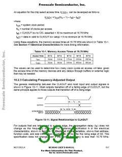
Figure 10-9. 8-bit Boot ROM Timing
10.2.2 Access Time Calculations
The two time paths that are critical in an MC68340 application using the CS≈ signals are
shown in Figure 10-10. The first path is the time from address valid to when data must be
available to the processor; the second path is the time from CS≈ asserted to when data
must be available to the processor.
S0
S1
S4
S5
S0
CLKOUT
A31–A0
t
6
t
9
CS
t
27
t
CSDV
D15–D0
t
ADV
Figure 10-10. Access Time Computation Diagram
As shown in the diagram, an equation for the address access time, t
developed as follows:
, can be
ADV
t
= t
(N – 0.5) – t – t
s9 s27
ADV cyc c
where:
t
= system CLKOUT period
cyc
N = number of clocks per bus cycle
c
t
= CLKOUT high to address valid = 30 ns maximum at 16.78 MHz
s6
t
= data-in valid to CLKOUT low setup = 5 ns minimum at 16.78 MHz
s27
10-6
MC68340 USER’S MANUAL
MOTOROLA
For More Information On This Product,
Go to: www.freescale.com

 FREESCALE [ Freescale ]