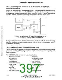
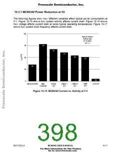
Freescale Semiconductor, Inc.
An equation for the chip select access time, t
, can be developed as follows:
CSDV
t
= t
(N – 1) – t – t
cyc c s9 s27
CSDV
where:
t
= system clock period
cyc
N = number of clocks per access
c
t
= CLKOUT low to CS≈ asserted = 30 ns maximum at 16.78 MHz
s9
t
= data-in valid to CLKOUT low setup = 5 ns minimum at 16.78 MHz
s27
Using these equations, the memory access times at 16.78 MHz are shown in Table 10-1.
See Section 11 Electrical Characteristics for more timing information.
Table 10-1. Memory Access Times at 16.78 MHz
Access Time
tADV
N = 2
54 ns
24 ns
N = 3
114 ns
84 ns
N = 4
173 ns
143 ns
N = 5
233 ns
203 ns
N = 6
292 ns
263 ns
tCSDV
The values can be used to determine how many clock cycles an access will take, given
the access time of the memory devices and any delays through buffers or external logic
that may be needed.
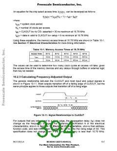
10.2.3 Calculating Frequency-Adjusted Output
The general relationship between the CLKOUT and most input and output signals is
shown in Figure 10-11. Most outputs transition off of a falling edge of CLKOUT, but the
same principle applies to those outputs that transition off of a rising edge.
CLKOUT
t
d
OUTPUTS
t
t
h
su
ASYNCHRONOUS
INPUTS
Figure 10-11. Signal Relationships to CLKOUT
For outputs that are referenced to a clock edge, the propagation delay (t ) does not
d
change as the frequency changes. For instance, specification 6 in the electrical
characteristics, shown in Section 11 Electrical Characteristics, shows that address,
function code, and size information is valid 3 to 30 ns after the rising edge of S0. This
specification does not change even if the device frequency is less than 16.78 MHz.
MOTOROLA
MC68340 USER’S MANUAL
10-7
For More Information On This Product,
Go to: www.freescale.com

 FREESCALE [ Freescale ]