Freescale Semiconductor, Inc.
includes a 3-bit instruction register without parity, consisting of a shift register with three
parallel outputs. Data is transferred from the shift register to the parallel outputs during the
update-IR controller state. The three bits are used to decode the four unique instructions
listed in Table 9-3.
The parallel output of the instruction register is reset to all ones in the test-logic-reset
controller state. Note that this preset state is equivalent to the BYPASS instruction.
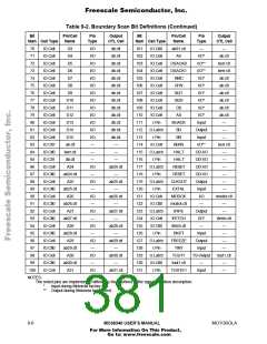
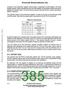
Table 9-3. Instructions
Code
Instruction
B2
0
B1
0
B0
0
EXTEST
SAMPLE/PRELOAD
BYPASS
0
0
1
X
1
1
X
0
0
HI-Z
1
0
1
BYPASS
During the capture-IR controller state, the parallel inputs to the instruction shift register are
loaded with the standard 2-bit binary value (01) into the two least significant bits and the
loss-of-crystal (LOC) status signal into bit 2. The parallel outputs, however, remain
unchanged by this action since an update-IR signal is required to modify them.
The LOC status bit of the instruction register indicates whether an internal clock is
detected when operating with a crystal clock source. The LOC bit is clear when a clock is
detected and set when it is not. The LOC bit is always clear when an external clock is
used. The LOC bit can be used to detect faulty connectivity when a crystal is used to clock
the device.
9.4.1 EXTEST (000)
The external test (EXTEST) instruction selects the 132-bit boundary scan register.
EXTEST asserts internal reset for the MC68340 system logic to force a predictable benign
internal state while performing external boundary scan operations.
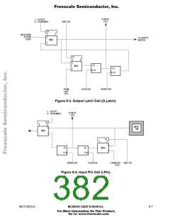
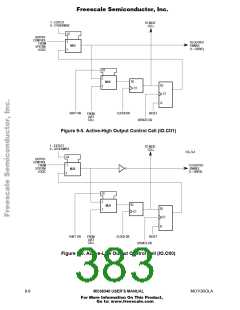
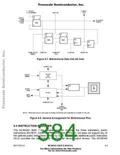
By using the TAP, the register is capable of a) scanning user-defined values into the
output buffers, b) capturing values presented to input pins, c) controlling the direction of
bidirectional pins, and d) controlling the output drive of three-state output pins. For more
details on the function and uses of EXTEST, please refer to the IEEE 1149.1 document.
9.4.2 SAMPLE/PRELOAD (001)
The SAMPLE/PRELOAD instruction selects the 132-bit boundary scan register and
provides two separate functions. First, it provides a means to obtain a snapshot of system
data and control signals. The snapshot occurs on the rising edge of TCK in the capture-
DR controller state. The data can be observed by shifting it transparently through the
boundary scan register.
9- 10
MC68340 USER’S MANUAL
MOTOROLA
For More Information On This Product,
Go to: www.freescale.com

 FREESCALE [ Freescale ]