Freescale Semiconductor, Inc.
NOTE
Since there is no internal synchronization between the IEEE
1149.1 clock (TCK) and the system clock (CLKOUT), the user
must provide some form of external synchronization to achieve
meaningful results.
The second function of SAMPLE/PRELOAD is to initialize the boundary scan register
output bits prior to selection of EXTEST. This initialization ensures that known data will
appear on the outputs when entering the EXTEST instruction.
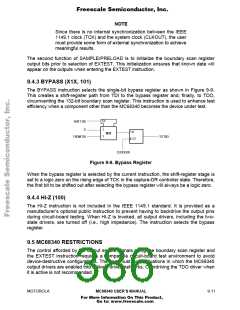
9.4.3 BYPASS (X1X, 101)
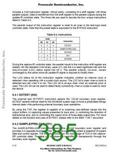
The BYPASS instruction selects the single-bit bypass register as shown in Figure 9-9.
This creates a shift-register path from TDI to the bypass register and, finally, to TDO,
circumventing the 132-bit boundary scan register. This instruction is used to enhance test
efficiency when a component other than the MC68340 becomes the device under test.
G1
SHIFT DR
0
1
1
1 D
C1
MUX
FROM TDI
TO TDO
CLOCK DR
Figure 9-9. Bypass Register
When the bypass register is selected by the current instruction, the shift-register stage is
set to a logic zero on the rising edge of TCK in the capture-DR controller state. Therefore,
the first bit to be shifted out after selecting the bypass register will always be a logic zero.
9.4.4 HI-Z (100)
The HI-Z instruction is not included in the IEEE 1149.1 standard. It is provided as a
manufacturer’s optional public instruction to prevent having to backdrive the output pins
during circuit-board testing. When HI-Z is invoked, all output drivers, including the two-
state drivers, are turned off (i.e., high impedance). The instruction selects the bypass
register.
9.5 MC68340 RESTRICTIONS
The control afforded by the output enable signals using the boundary scan register and
the EXTEST instruction requires a compatible circuit-board test environment to avoid
device-destructive configurations. The user must avoid situations in which the MC68340
output drivers are enabled into actively driven networks. Overdriving the TDO driver when
it is active is not recommended.
MOTOROLA
MC68340 USER’S MANUAL
9- 11
For More Information On This Product,
Go to: www.freescale.com

 FREESCALE [ Freescale ]