Freescale Semiconductor, Inc.
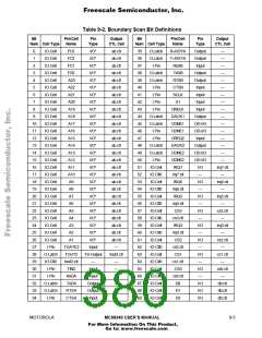
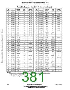
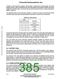
Table 9-2. Boundary Scan Bit Definitions (Continued)
Bit
Pin/Cell
Name
Pin
Type
Output
CTL Cell
Bit
Pin/Cell
Name
Pin
Type
Output
CTL Cell
Num Cell Type
Num Cell Type
70
71
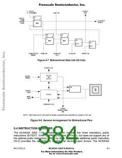
IO.Cell
IO.Cell
IO.Cell
IO.Cell
IO.Cell
IO.Cell
IO.Cell
IO.Cell
IO.Cell
IO.Cell
IO.Cell
IO.Cell
IO.Cell
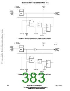
IO.Ctl1
IO.Ctl0
IO.Ctl1
IO.Cell
IO.Ctl0
IO.Cell
IO.Ctl0
IO.Cell
IO.Ctl0
IO.Cell
IO.Ctl0
IO.Cell
IO.Ctl0
IO.Cell
IO.Ctl0
IO.Cell
IO.Ctl0
IO.Cell
D3
D4
I/O
I/O
I/O
I/O
I/O
I/O
I/O
I/O
I/O
I/O
I/O
I/O
I/O
—
db.ctl
db.ctl
db.ctl
db.ctl
db.ctl
db.ctl
db.ctl
db.ctl
db.ctl
db.ctl
db.ctl
db.ctl
db.ctl
—
101
102
103
104
105
106
107
108
109
110
111
112
113
114
115
116
117
118
119
120
121
122
123
124
125
126
127
128
129
130
131
IO.Ctl0
IO.Cell
IO.Cell
IO.Cell
IO.Cell
IO.Cell
IO.Cell
IO.Cell
IO.Cell
IO.Cell
I.Pin
ab31.ctl
A0
—
I/O*
—
ab.ctl
berr.ctl
berr.ctl
ab.ctl
ab.ctl
ab.ctl
ab.ctl
ab.ctl
ab.ctl
—
72
D5
DSACK0
DSACK1
RMC
I/O**
I/O**
I/O*
73
D6
74
D7
75
D8
R/W
I/O*
76
D9
SIZ1
I/O*
77
D10
SIZ0
I/O*
78
D11
DS
I/O*
79
D12
AS
I/O*
80
D13
BGACK
BG
Input
Output
Input
I/O**
OD-I/O
OD-I/O
OD-I/O
OD-I/O
Output
Input
I/O
81
D14
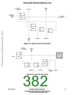
O.Latch
I.Pin
—
82
D15
BR
—
83
ab.ctl
berr.ctl
db.ctl
A24
IO.Cell
O.Latch
I.Pin
BERR
berr.ctl
—
84
—
—
HALT
HALT
RESET
RESET
CLKOUT
EXTAL
MODCK
modck.ctl
IPIPE
85
—
—
—
86
I/O
—
ab24.ctl
—
O.Latch
I.Pin
—
87
ab24.ctl
A25
—
88
I/O
—
ab25.ctl
—
O.Latch
I.Pin
—
89
ab25.ctl
A26
—
90
I/O
—
ab26.ctl
—
IO.Cell
IO.Ctl0
O.Latch
IO.Cell
IO.Ctl0
I.Pin
modck.ctl
—
91
ab26.ctl
A27
—
92
I/O
—
ab27.ctl
—
Output
I/O*
—
93
ab27.ctl
A28
IFETCH
ifetch.ctl
BKPT
FREEZE
TIN1
ifetch.ctl
—
94
I/O
—
ab28.ctl
—
—
95
ab28.ctl
A29
Input
Output
Input
TS-Output
—
—
96
I/O
—
ab29.ctl
—
O.Latch
I.Pin
—
97
ab29.ctl
A30
—
98
I/O
—
ab30.ctl
—
O.Latch
IO.Ctl0
I.Pin
TOUT1
tout1.ctl
TGATE1
tout1.ctl
—
99
ab30.ctl
A31
100
I/O
ab31.ctl
Input
—
NOTES:
The noted pins are implemented differently than defined in the signal definition description:
Input during Motorola factory test
** Output during Motorola factory test
*
9- 6
MC68340 USER’S MANUAL
MOTOROLA
For More Information On This Product,
Go to: www.freescale.com

 FREESCALE [ Freescale ]