Freescale Semiconductor, Inc.
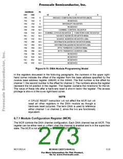
ADDRESS
CH1
FC
CH2
7A0
7A2
7A4
7A6
7A8
7AA
7AC
7AE
7B0
7B2
7B4
7B6
7B8
7BA
7BC
7BE
15
8
7
0
780
782
784
786
788
78A
78C
78E
790
792
794
796
798
79A
79C
79E
S
MODULE CONFIGURATION REGISTER (MCR)
RESERVED
S
S
INTERRUPT REGISTER
RESERVED
S/U
S/U
S/U
S/U
S/U
S/U
S/U
S/U
S/U
S/U
S/U
S/U
S/U
CHANNEL CONTROL REGISTER
CHANNEL STATUS REGISTER
FUNCTION CODE REGISTER
SOURCE ADDRESS REGISTER MSBs
SOURCE ADDRESS REGISTER LSBs
DESTINATION ADDRESS REGISTER MSBs
DESTINATION ADDRESS REGISTER LSBs
BYTE TRANSFER COUNTER MSBs
BYTE TRANSFER COUNTER LSBs
RESERVED
RESERVED
RESERVED
RESERVED
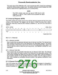
Figure 6-15. DMA Module Programming Model
In the registers discussed in the following paragraphs, the numbers in the upper right-
hand corner indicate the offset of the register from the base address specified by the
module base address register (MBAR) in the SIM40. The first number is the offset for
channel 1; the second number is the offset for channel 2. The numbers above the register
represent the bit position in the register. The register contains the mnemonic for the bit.
The value of these bits after a hardware reset is shown below the register. The access
privilege is shown in the lower right-hand corner.
NOTE
A CPU32 RESET instruction will not affect the MCR but will
reset all other registers in the DMA module as though a
hardware reset occurred. The term DMA is used to reference
either channel 1 or channel 2, since the two are functionally
equivalent.
6.7.1 Module Configuration Register (MCR)
The MCR controls the DMA channel configuration. Each DMA channel has an MCR. This
register can be either read or written when the channel is enabled and is in the supervisor
state. The MCR is not affected by a CPU32 RESET instruction.
MOTOROLA
MC68340 USER’S MANUAL
6- 23
For More Information On This Product,
Go to: www.freescale.com

 FREESCALE [ Freescale ]