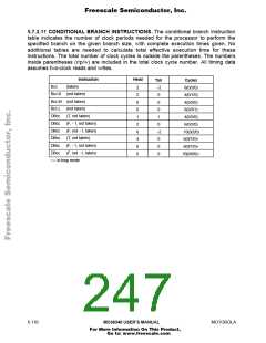
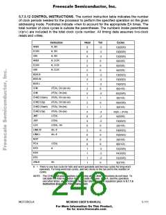
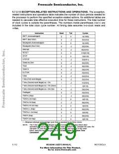
Freescale Semiconductor, Inc.
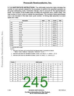
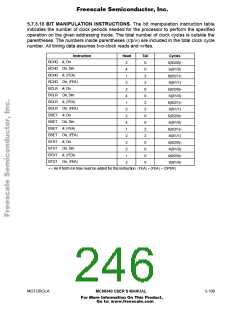
5.7.3.10 BIT MANIPULATION INSTRUCTIONS. The bit manipulation instruction table
indicates the number of clock periods needed for the processor to perform the specified
operation on the given addressing mode. The total number of clock cycles is outside the
parentheses. The numbers inside parentheses (r/p/w) are included in the total clock cycle
number. All timing data assumes two-clock reads and writes.
Instruction
Head
Tail
0
Cycles
6(0/2/0)
6(0/1/0)
8(0/2/1)
8(0/1/1)
6(0/2/0)
6(0/1/0)
8(0/2/1)
8(0/1/1)
6(0/2/0)
6(0/1/0)
8(0/2/1)
8(0/1/1)
4(0/2/0)
4(0/1/0)
4(0/2/0)
8(0/1/0)
BCHG #, Dn
2
4
1
2
2
4
1
2
2
4
1
2
2
2
1
2
BCHG Dn, Dm
BCHG #, FEA
BCHG Dn, FEA
BCLR #, Dn
0
2
2
0
BCLR Dn, Dm
BCLR #, FEA
BCLR Dn, FEA
BSET #, Dn
0
2
2
0
BSET Dn, Dm
BSET #, FEA
BSET Dn, FEA
BTST #, Dn
0
2
2
0
BTST Dn, Dm
BTST #, FEA
BTST Dn, FEA
0
0
0
= An # fetch EA time must be added for this instruction: FEA + FEA + OPER
MOTOROLA
MC68340 USER’S MANUAL
5-109
For More Information On This Product,
Go to: www.freescale.com

 FREESCALE [ Freescale ]