Freescale Semiconductor, Inc.
Development Support
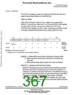
Background Debug Mode
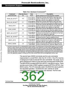
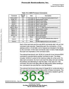
Table 18-3. BDM Firmware Commands
Opcode
Command
Data
Description
(Hex)
62
63
64
65
66
67
42
43
44
45
46
47
08
READ_NEXT
READ_PC
READ_D
16-bit data out X = X + 2; Read next word pointed to by X
16-bit data out Read program counter
16-bit data out Read D accumulator
16-bit data out Read X index register
16-bit data out Read Y index register
16-bit data out Read stack pointer
READ_X
READ_Y
READ_SP
WRITE_NEXT
WRITE_PC
WRITE_D
WRITE_X
WRITE_Y
WRITE_SP
GO
16-bit data in X = X + 2; Write next word pointed to by X
16-bit data in Write program counter
16-bit data in Write D accumulator
16-bit data in Write X index register
16-bit data in Write Y index register
16-bit data in Write stack pointer
None
None
None
Go to user program
Execute one user instruction then return to
BDM
TRACE1
TAGGO
10
18
Enable tagging and go to user program
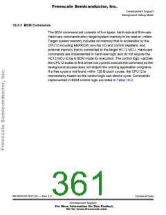
Each of the hardware and firmware BDM commands start with an 8-bit
command code (opcode). Depending upon the commands, a 16-bit
address and/or a 16-bit data word is required as indicated in the tables
by the command. All the read commands output 16-bits of data despite
the byte/word implication in the command name.
The external host should wait 150 BCLK cycles for a non-intrusive BDM
command to execute before another command is sent. This delay
includes 128 BCLK cycles for the maximum delay for a free cycle. For
data read commands, the host must insert this delay between sending
the address and attempting to read the data. In the case of a write
command, the host must delay after the data portion before sending a
new command to be sure that the write has finished.
The external host should delay about 32 target BCLK cycles between a
firmware read command and the data portion of these commands. This
allows the BDM firmware to execute the instructions needed to get the
requested data into the BDM SHIFTER register.
MC68HC912DG128 — Rev 3.0
Technical Data
Development Support
For More Information On This Product,
Go to: www.freescale.com

 FREESCALE [ Freescale ]