Freescale Semiconductor, Inc.
Development Support
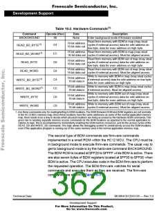
In special single-chip mode, background operation is enabled and active
immediately out of reset. This active case replaces the M68HC11 boot
function, and allows programming a system with blank memory.
While BDM is active, a set of BDM control registers are mapped to
addresses $FF00 to $FF06. The BDM control logic uses these registers
which can be read anytime by BDM logic, not user programs. Refer to
BDM Registers for detailed descriptions.
Some on-chip peripherals have a BDM control bit which allows
suspending the peripheral function during BDM. For example, if the timer
control is enabled, the timer counter is stopped while in BDM. Once
normal program flow is continued, the timer counter is re-enabled to
simulate real-time operations.
18.4.2 BDM Serial Interface
The BDM serial interface requires the external controller to generate a
falling edge on the BKGD pin to indicate the start of each bit time. The
external controller provides this falling edge whether data is transmitted
or received.
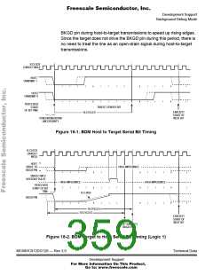
BKGD is a pseudo-open-drain pin that can be driven either by an
external controller or by the MCU. Data is transferred MSB first at 16 B-
clock cycles per bit (nominal speed). The interface times out if 512 B-
clock cycles occur between falling edges from the host. The hardware
clears the command register when a time-out occurs.
The BKGD pin can receive a high or low level or transmit a high or low
level. The following diagrams show timing for each of these cases.
Interface timing is synchronous to MCU clocks but asynchronous to the
external host. The internal clock signal is shown for reference in counting
cycles.
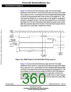
Figure 18-1 shows an external host transmitting a logic one or zero to the
BKGD pin of a target MC68HC912DG128 MCU. The host is
asynchronous to the target so there is a 0-to-1 cycle delay from the host-
generated falling edge to where the target perceives the beginning of the
bit time. Ten target B cycles later, the target senses the bit level on the
BKGD pin. Typically the host actively drives the pseudo-open-drain
Technical Data
MC68HC912DG128 — Rev 3.0
Development Support
For More Information On This Product,
Go to: www.freescale.com

 FREESCALE [ Freescale ]