Freescale Semiconductor, Inc.
Timer Interface Module (TIM)
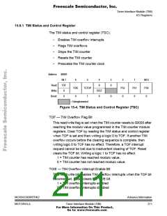
Functional Description
15.5.9 PWM Initialization
To ensure correct operation when generating unbuffered or buffered
PWM signals, use this initialization procedure:
1. In the TIM status and control register (TSC):
a. Stop the TIM counter by setting the TIM stop bit, TSTOP.
b. Reset the TIM counter by setting the TIM reset bit, TRST.
2. In the TIM counter modulo registers (TMODH and TMODL), write
the value for the required PWM period.
3. In the TIM channel x registers (TCHxH and TCHxL), write the
value for the required pulse width.
4. In TIM channel x status and control register (TSCx):
a. Write 0:1 (for unbuffered output compare or PWM signals) or
1:0 (for buffered output compare or PWM signals) to the
mode select bits, MSxB and MSxA. See Table 15-3.
b. Write 1 to the toggle-on-overflow bit, TOVx.
c. Write 1:0 (to clear output on compare) or 1:1 (to set output on
compare) to the edge/level select bits, ELSxB and ELSxA.
The output action on compare must force the output to the
complement of the pulse width level. See Table 15-3.
NOTE: In PWM signal generation, do not program the PWM channel to toggle
on output compare. Toggling on output compare prevents reliable
0 percent duty cycle generation and removes the ability of the channel
to self-correct in the event of software error or noise. Toggling on output
compare can also cause incorrect PWM signal generation when
changing the PWM pulse width to a new, much larger value.
5. In the TIM status control register (TSC), clear the TIM stop bit,
TSTOP.
Setting MS0B links channels 0 and 1 and configures them for buffered
PWM operation. The TIM channel 0 registers (TCH0H and TCH0L)
initially control the buffered PWM output. TIM status control register 0
(TSCR0) controls and monitors the PWM signal from the linked
channels.
MC68HC908RFRK2
MOTOROLA
AdvanceInformation
207
Timer Interface Module (TIM)
For More Information On This Product,
Go to: www.freescale.com

 FREESCALE [ Freescale ]