Freescale Semiconductor, Inc.
Timer Interface Module (TIM)
15.8.1 TIM Clock Pin (TCLK)
TCLK is an external clock input that can be the clock source for the TIM
counter instead of the prescaled internal bus clock. Select the TCLK
input by writing logic 1s to the three prescaler select bits, PS2–PS0. See
15.9.1 TIM Status and Control Register. The minimum TCLK pulse
width, TCLKLMIN or TCLKHMIN, is:
1
+ t
su
bus frequency
The maximum TCLK frequency is:
bus frequency ÷ 2
Refer to 17.10 Control Timing.
TCLK is available as a general-purpose I/O pin when not used as the
TIM clock input. When the TCLK pin is the TIM clock input, it is an input
regardless of the state of the DDRB3 bit in data direction register B.
15.8.2 TIM Channel I/O Pins (TCH0)
The channel I/O pins are programmable independently as an input
capture pin or an output compare pin. TCH0 can be configured as
buffered output compare or buffered PWM pins.
15.9 I/O Registers
These I/O registers control and monitor operation of the TIM:
•
•
•
•
•
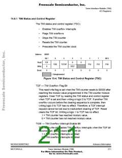
TIM status and control register, TSC
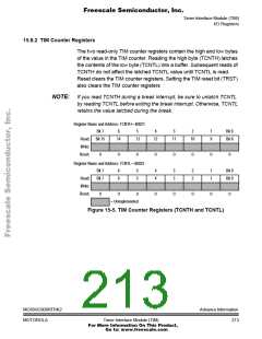
TIM control registers, TCNTH and TCNTL
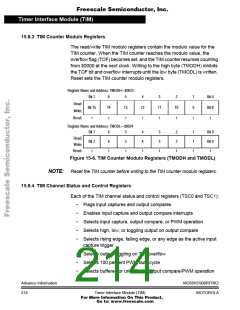
TIM counter modulo registers, TMODH and TMODL
TIM channel status and control registers, TSC0 and TSC1
TIM channel registers, TCH0H, TCH0L, TCH1H, and TCH1L
Advance Information
210
MC68HC908RFRK2
MOTOROLA
Timer Interface Module (TIM)
For More Information On This Product,
Go to: www.freescale.com

 FREESCALE [ Freescale ]