Freescale Semiconductor, Inc.
Timer Interface Module (TIM)
Functional Description
An unsynchronized write to the TIM channel registers to change an
output compare value could cause incorrect operation for up to two
counter overflow periods. For example, writing a new value before the
counter reaches the old value but after the counter reaches the new
value prevents any compare during that counter overflow period. Also,
using a TIM overflow interrupt routine to write a new, smaller output
compare value may cause the compare to be missed. The TIM may pass
the new value before it is written.
Use these methods to synchronize unbuffered changes in the output
compare value on channel x:
•
When changing to a smaller value, enable channel x output
compare interrupts and write the new value in the output compare
interrupt routine. The output compare interrupt occurs at the end
of the current output compare pulse. The interrupt routine has until
the end of the counter overflow period to write the new value.
•
When changing to a larger output compare value, enable channel
x TIM overflow interrupts and write the new value in the TIM
overflow interrupt routine. The TIM overflow interrupt occurs at the
end of the current counter overflow period. Writing a larger value
in an output compare interrupt routine (at the end of the current
pulse) could cause two output compares to occur in the same
counter overflow period.
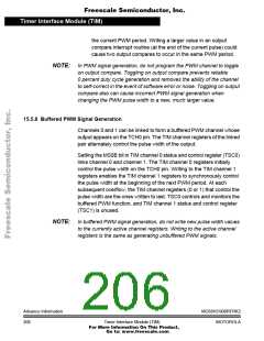
15.5.5 Buffered Output Compare
Channels 0 and 1 can be linked to form a buffered output compare
channel whose output appears on the PTB2/TCH0 pin. The TIM channel
registers of the linked pair alternately control the output.
Setting the MS0B bit in TIM channel 0 status and control register (TSC0)
links channel 0 and channel 1. The output compare value in the TIM
channel 0 registers initially controls the output on the TCH0 pin. Writing
to the TIM channel 1 registers enables the TIM channel 1 registers to
synchronously control the output after the TIM overflows. At each
subsequent overflow, the TIM channel registers (0 or 1) that control the
output are the ones written to last. TSC0 controls and monitors the
MC68HC908RFRK2
MOTOROLA
AdvanceInformation
Timer Interface Module (TIM)
203
For More Information On This Product,
Go to: www.freescale.com

 FREESCALE [ Freescale ]