Signal Pins
Table 2-2 Signal and Package Information for the 128-Pin LQFP
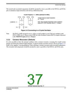
State
During
Reset
Signal
Name
Pin No.
Type
Signal Description
ANA4
ANA5
ANA6
ANA7
VREFH
84
85
86
87
93
Input
Analog
Input
ANA4 - 7 — Analog inputs to ADC A, channel 1
Input
Analog
Input
VREFH — Analog Reference Voltage High. VREFH must be less
than or equal to VDDA_ADC.
VREFP
VREFMID
VREFN
92
91
90
89
Input/
Output
Analog
Input/
Output
VREFP, VREFMID & VREFN — Internal pins for voltage reference
which are brought off-chip so that they can be bypassed.
Connect to a 0.1 μF low ESR capacitor.
VREFLO
Input
Input
Analog
Input
VREFLO — Analog Reference Voltage Low. This should normally
be connected to a low-noise VSSA
.
ANB0
ANB1
ANB2
ANB3
ANB4
ANB5
ANB6
ANB7
96
97
Analog
Input
ANB0 - 3 — Analog inputs to ADC B, channel 0
98
99
100
101
102
103
88
Input
Analog
Input
ANB4 - 7 — Analog inputs to ADC B, channel 1
TEMP_
SENSE
Output
Analog
Output
Temperature Sense Diode — This signal connects to an
on-chip diode that can be connected to one of the ADC inputs
and is used to monitor the temperature of the die. Must be
bypassed with a 0.01 μF capacitor.
CAN_RX
121
Schmitt
Input
Input,
pull-up
enabled
FlexCAN Receive Data — This is the CAN input. This pin has
an internal pull-up resistor.
To deactivate the internal pull-up resistor, set the CAN bit in the
SIM_PUDR register.
56F8345 Technical Data, Rev. 17
Freescale Semiconductor
Preliminary
33

 FREESCALE [ Freescale ]