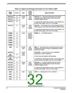
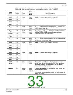
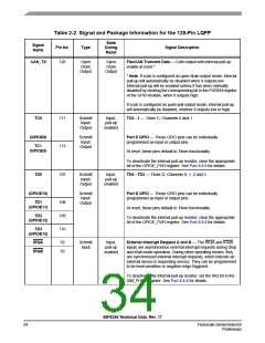
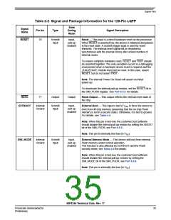
Table 2-2 Signal and Package Information for the 128-Pin LQFP
State
During
Reset
Signal
Name
Pin No.
Type
Signal Description
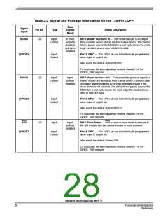
FAULTA0
FAULTA1
FAULTA2
67
68
69
Schmitt
Input
Input,
pull-up
enabled
FAULTA0 - 2 — These three fault input pins are used for
disabling selected PWMA outputs in cases where fault
conditions originate off-chip.
To deactivate the internal pull-up resistor, set the PWMA0 bit in
the SIM_PUDR register. See Part 6.5.6 for details.
FAULTA3
70
Schmitt
Input
Input,
pull-up
enabled
FAULTA3 — This fault input pin is used for disabling selected
PWMA outputs in cases where fault conditions originate off-chip.
To deactivate the internal pull-up resistor, set the PWMA1 bit in
the SIM_PUDR register. See Part 6.5.6 for details.
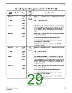
PWMB0
PWMB1
PWMB2
PWMB3
PWMB4
PWMB5
ISB0
32
33
34
37
38
39
48
Output
In reset,
output is
disabled,
pull-up is
enabled
PWMB0 - 5 — Six PWMB output pins.
Schmitt
Input
Input,
pull-up
enabled
ISB0 - 2 — These three input current status pins are used for
top/bottom pulse width correction in complementary channel
operation for PWMB.
(GPIOD10)
Schmitt
Input/
Output
Port D GPIO — These GPIO pins can be individually
programmed as input or output pins.
ISB1
(GPIOD11)
50
51
At reset, these pins default to ISB functionality.
ISB2
(GPIOD12)
To deactivate the internal pull-up resistor, clear the appropriate
bit of the GPIOD_PUR register. See Part 6.5.6 for details.
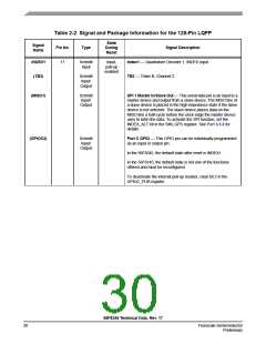
FAULTB0
FAULTB1
FAULTB2
FAULTB3
ANA0
54
55
56
57
80
81
82
83
Schmitt
Input
Input,
pull-up
enabled
FAULTB0 - 3 — These four fault input pins are used for
disabling selected PWMB outputs in cases where fault
conditions originate off-chip.
To deactivate the internal pull-up resistor, set the PWMB bit in
the SIM_PUDR register. See Part 6.5.6 for details.
Input
Analog
Input
ANA0 - 3 — Analog inputs to ADC A, channel 0
ANA1
ANA2
ANA3
56F8345 Technical Data, Rev. 17
32
Freescale Semiconductor
Preliminary

 FREESCALE [ Freescale ]