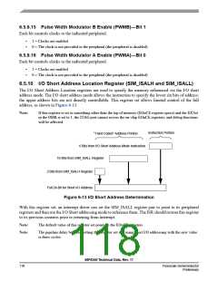
7.2 Flash Access Blocking Mechanisms
The 56F8345/56F8145 have several operating functional and test modes. Effective Flash security must
address operating mode selection and anticipate modes in which the on-chip Flash can be compromised
and read without explicit user permission. Methods to block these are outlined in the next subsections.
7.2.1
Forced Operating Mode Selection
At boot time, the SIM determines in which functional modes the device will operate. These are:
•
•
Unsecured Mode
Secure Mode (EOnCE disabled)
When Flash security is enabled as described in the Flash Memory module specification, the device will
disable the EOnCE debug interface.
7.2.2
Disabling EOnCE Access
On-chip Flash can be read by issuing commands across the EOnCE port, which is the debug interface for
the 56800E core. The TRST, TCLK, TMS, TDO, and TDI pins comprise a JTAG interface onto which the
EOnCE port functionality is mapped. When the device boots, the chip-level JTAG TAP (Test Access Port)
is active and provides the chip’s boundary scan capability and access to the ID register.
Proper implementation of Flash security requires that no access to the EOnCE port is provided when
security is enabled. The 56800E core has an input which disables reading of internal memory via the
JTAG/EOnCE. The FM sets this input at reset to a value determined by the contents of the FM security
bytes.
7.2.3
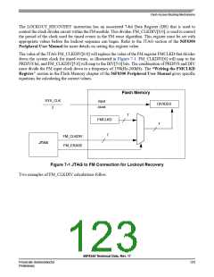
Flash Lockout Recovery
If a user inadvertently enables Flash security on the device, a built-in lockout recovery mechanism can be
used to reenable access to the device. This mechanism completely reases all on-chip Flash, thus disabling
Flash security. Access to this recovery mechanism is built into CodeWarrior via an instruction in memory
configuration (.cfg) files. Add, or uncomment the following configuration command:
unlock_flash_on_connect 1
For more information, please see CodeWarrior MC56F83xx/DSP5685x Family Targeting Manual.
56F8345 Technical Data, Rev. 17
122
Freescale Semiconductor
Preliminary

 FREESCALE [ Freescale ]