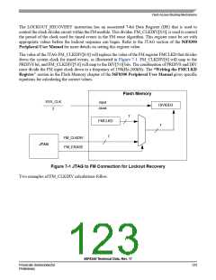
Flash Access Blocking Mechanisms
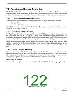
The LOCKOUT_RECOVERY instruction has an associated 7-bit Data Register (DR) that is used to
control the clock divider circuit within the FM module. This divider, FM_CLKDIV[6:0], is used to control
the period of the clock used for timed events in the FM erase algorithm. This register must be set with
appropriate values before the lockout sequence can begin. Refer to the JTAG section of the 56F8300
Peripheral User Manual for more details on setting this register value.
The value of the JTAG FM_CLKDIV[6:0] will replace the value of the FM register FMCLKD that divides
down the system clock for timed events, as illustrated in Figure 7-1. FM_CLKDIV[6] will map to the
PRDIV8 bit, and FM_CLKDIV[5:0] will map to the DIV[5:0] bits. The combination of PRDIV8 and DIV
must divide the FM input clock down to a frequency of 150kHz-200kHz. The “Writing the FMCLKD
Register” section in the Flash Memory chapter of the 56F8300 Peripheral User Manual gives specific
equations for calculating the correct values.
Flash Memory
SYS_CLK
2
input
clock
DIVIDER
7
FMCLKD
7
7
FM_CLKDIV
FM_ERASE
JTAG
Figure 7-1 JTAG to FM Connection for Lockout Recovery
Two examples of FM_CLKDIV calculations follow.
56F8345 Technical Data, Rev. 17
Freescale Semiconductor
Preliminary
123

 FREESCALE [ Freescale ]