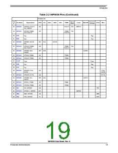
56F8036 Signal Pins
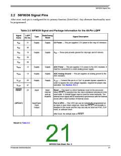
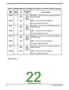
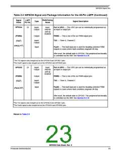
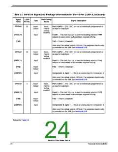
Table 2-3 56F8036 Signal and Package Information for the 48-Pin LQFP (Continued)
Signal
Name
LQFP
Pin No.
StateDuring
Reset
Type
Signal Description
GPIOA4
33
Input/
Output
Input,
internal
pull-up
enabled
Port A GPIO — This GPIO pin can be individually programmed as
an input or output pin.
(PWM4)
(TA21)
Output
PWM4 — This is one of the six PWM output pins.
TA2 — Timer A, Channel 2
Input/
Output
(FAULT12)
Input
Fault1 — This fault input pin is used for disabling selected PWM
outputs in cases where fault conditions originate off-chip.
After reset, the default state is GPIOA4. The peripheral functionality
is controlled via the SIM. See Section 6.3.16.
1The TA2 signal is also brought out on the GPIOA8-9 and GPIOB2-3 pins.
2The Fault1 signal is also brought out on the GPIOA8-9 and GPIOB10 pins.
GPIOA5
29
Input/
Output
Input,
internal
pull-up
enabled
Port A GPIO — This GPIO pin can be individually programmed as
an input or output pin.
(PWM5)
(TA33)
Output
PWM5 — This is one of the six PWM output pins.
TA3 — Timer A, Channel 3
Input/
Output
Input
Fault2 — This fault input pin is used for disabling selected PWM
outputs in cases where fault conditions originate off-chip.
(FAULT24)
After reset, the default state is GPIOA5. The peripheral functionality
is controlled via the SIM. See Section 6.3.16.
3The TA3 signal is also brought out on the GPIOA8-9 and GPIOB2-3 pins.
4The Fault2 signal is also brought out on the GPIOA8-9 and GPIOB10 pins.
Return to Table 2-2
56F8036 Data Sheet, Rev. 6
Freescale Semiconductor
23

 FREESCALE [ Freescale ]