56F8036 Signal Pins
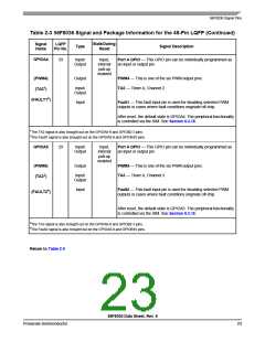
Table 2-3 56F8036 Signal and Package Information for the 48-Pin LQFP (Continued)
Signal
Name
LQFP
Pin No.
StateDuring
Reset
Type
Signal Description
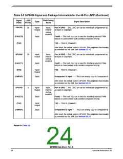
GPIOB5
4
Input/
Output
Input,
internal
pull-up
enabled
Port B GPIO — This GPIO pin can be individually programmed as
an input or output pin.
(TA1)
Input/
TA1 — Timer A, Channel 1
Output
(FAULT3)
(CLKIN)
Input
Input
FAULT3 — This fault input pin is used for disabling selected PWM
outputs in cases where fault conditions originate off-chip.
External Clock Input— This pin serves as an external clock input.
After reset, the default state is GPIOB5. The peripheral functionality
is controlled via the SIM. See Section 6.3.16.
GPIOB6
1
Input/
Output
Input,
internal
pull-up
enabled
Port B GPIO — This GPIO pin can be individually programmed as
an input or output pin.
(RXD0)
(SDA9)
Input
Receive Data 0 — QSCI0 receive data input.
Serial Data — This pin serves as the I2C serial data line.
Input/
Output
Input
(CLKIN)
External Clock Input — This pin serves as an external clock input.
After reset, the default state is GPIOB6. The peripheral functionality
is controlled via the SIM (See Section 6.3.16) and the CLKMODE bit
of the OCCS Oscillator Control Register.
9The SDA signal is also brought out on the GPIOB1 pin.
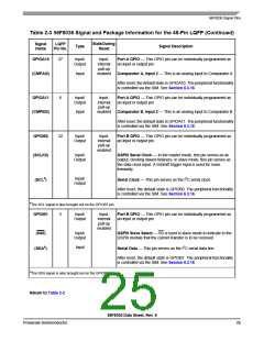
GPIOB7
3
Input/
Output
Input,
internal
pull-up
enabled
Port B GPIO — This GPIO pin can be individually programmed as
an input or output pin.
(TXD0)
Input/
Transmit Data 0 — QSCI0 transmit data output or transmit / receive
Output
in single wire operation.
(SCL10
)
Serial Clock — This pin serves as the I2C serial clock.
Input/
Output
After reset, the default state is GPIOB7. The peripheral functionality
is controlled via the SIM. See Section 6.3.16.
10The SCL signal is also brought out on the GPIOB0 pin.
Return to Table 2-2
56F8036 Data Sheet, Rev. 6
Freescale Semiconductor
27

 FREESCALE [ Freescale ]