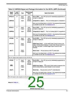
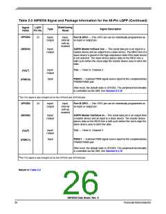
Table 2-3 56F8036 Signal and Package Information for the 48-Pin LQFP (Continued)
Signal
Name
LQFP
Pin No.
StateDuring
Reset
Type
Signal Description
GPIOB2
25
Input/
Output
Input,
internal
pull-up
enabled
Port B GPIO — This GPIO pin can be individually programmed as
an input or output pin.
(MISO0)
Input/
Output
QSPI0 Master In/Slave Out — This serial data pin is an input to a
master device and an output from a slave device. The MISO line of a
slave device is placed in the high-impedance state if the slave device
is not selected. The slave device places data on the MISO line a
half-cycle before the clock edge the master device uses to latch the
data.
(TA27)
Input/
Output
TA2 — Timer A, Channel 2
Input
PSRC0 — External PWM signal source input for the complementary
PWM4/PWM5 pair.
(PSRC0)
After reset, the default state is GPIOB2. The peripheral functionality
is controlled via the SIM. See Section 6.3.16.
7The TA2 signal is also brought out on the GPIOA4 and GPIOA8 pins.
GPIOB3
24
Input/
Output
Input,
internal
pull-up
enabled
Port B GPIO — This GPIO pin can be individually programmed as
an input or output pin.
(MOSI0)
Input/
Output
QSPI0 Master Out/Slave In— This serial data pin is an output from
a master device and an input to a slave device. The master device
places data on the MOSI line a half-cycle before the clock edge the
slave device uses to latch the data.
(TA38)
Input/
Output
TA3 — Timer A, Channel 3
Input
PSRC1 — External PWM signal source input for the complementary
PWM2/PWM3 pair.
(PSRC1)
After reset, the default state is GPIOB3. The peripheral functionality
is controlled via the SIM. See Section 6.3.16.
8The TA3 signal is also brought out on the GPIOA5 and GPIOA9 pins.
Return to Table 2-2
56F8036 Data Sheet, Rev. 6
26
FreescaleSemiconductor

 FREESCALE [ Freescale ]