The user is responsible for directing the device to invoke the flash programming subroutine to reprogram
the word $0000 into program memory location $00 7FF7. This is done by, for example, toggling a specific
pin or downloading a user-defined key through serial interfaces.
Note:
Flash contents can only be programmed for 1s to 0s.
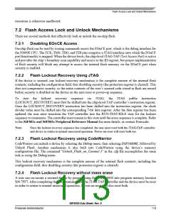
7.3 Product Analysis
The recommended method of unsecuring a secured device for product analysis of field failures is via the
method described in section 7.2.4. The customer would need to supply Technical Support with the details
of the protocol to access the subroutines in flash memory. An alternative method for performing analysis
on a secured device would be to mass-erase and reprogram the flash with the original code, but modify the
security word or not program the security word.
Part 8 General Purpose Input/Output (GPIO)
8.1 Introduction
This section is intended to supplement the GPIO information found in the 56F802X and
56F803XPeripheral Reference Manual and contains only chip-specific information. This information
supersedes the generic information in the 56F802X and 56F803XPeripheral Reference Manual.
8.2 Configuration
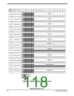
There are four GPIO ports defined on the 56F8036. The width of each port, the associated peripheral and
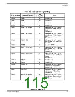
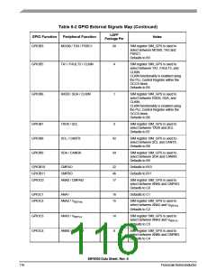
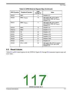
reset functions are shown in Table 8-1. The specific mapping of GPIO port pins is shown in Table 8-2.
Additional details are shown in Tables 2-2 and 2-3.
Table 8-1 GPIO Ports Configuration
Available
GPIO Port
Pins in
Peripheral Function
Reset Function
56F8036
PWM, Timer, QSPI, Comparator, Reset
GPIO, RESET
A
B
12
11
QSPI, I2C, PWM, Clock, MSCAN,
Comparator, Timer
GPIO
ADC, Comparator, QSCI
GPIO
C
D
10
6
Clock, Oscillator, DAC, JTAG
GPIO, JTAG
56F8036 Data Sheet, Rev. 6
114
FreescaleSemiconductor

 FREESCALE [ Freescale ]