Clocks
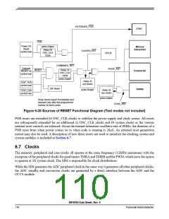
The deassertion sequence of internal resets coordinates the device start up, including the clocking system
start up. The sequence is described in the following steps:
1. As power is applied, the Relaxation Oscillator starts to operate. When a valid operating voltage is
reached, the POR reset will release.
2. The release of POR reset permits operation of the POR reset extender. The POR extender generates
an extended POR reset, which is released 64 OSC_CLK cycles after POR reset. This provides an
additional time period for the clock source and power to stabilize.
3. A Combined reset consists of the OR of the extended POR reset, the external reset, the COP reset
and Software reset. The entire device, except for the POR extender, is held reset as long as
Combined reset is asserted. The release of Combined reset permits operation of the CTRL register,
the Synchronous reset generator, and the CLKGEN reset extender.
4. The Synchronous reset generator generates a reset to the Software and COP reset logic. The COP
and Software reset logic is released three OSC_CLK cycles after Combined reset deasserts. This
provides a reasonable minimum duration to the reset for these specialized functions.
5. The CLKGEN reset extender generates the CLKGEN reset used by the clock generation logic. The
CLKGEN reset is released 32 OSC_CLK cycles after Combined reset deasserts. This provides a
window in which the SIM stabilizes the master clock inputs to the clock generator.
6. The release of CLKGEN reset permits operation of the clock generation logic and the Peripheral
reset extender. The Peripheral reset extender generates the Peripheral reset, which is released 32
SYS_CLK cycles after CLKGEN reset. This provides a window in which peripheral and core logic
remain clocked, but in reset, so that synchronous resets can be resolved.
7. The release of Peripheral reset permits operation of the peripheral logic and the Core reset extender.
The Core reset extender generates the Core reset, which is released 32 SYS_CLK cycles after the
Peripheral reset. This provides a window in which critical peripheral start-up functions, such as
Flash Security in the Flash memory, can be implemented.
8. The release of Core reset permits execution of code by the 56800E core and marks the end of the
system start-up sequence.
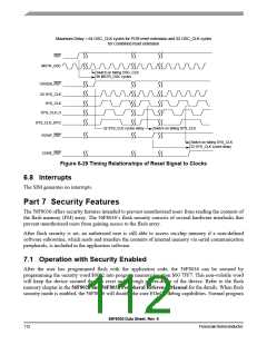
Figure 6-29 illustrates clock relationships to one another and to the various resets as the device comes out
of reset. RST is assumed to be the logical AND of all active-low system resets (for example, POR, external
reset, COP and Software reset). In the 56F8036, this signal will be stretched by the SIM for a period of
time (up to 96 OSC_CLK clock cycles, depending upon the status of the POR) to create the clock
generation reset signal (CLKGEN_RST). The SIM should deassert CLKGEN_RST synchronously with
the negative edge of OSC_CLK in order to avoid skew problems. CLKGEN_RST is delayed 32 SYS_CLK
cycles to create the peripheral reset signal (PERIP_RST). PERIP_RST is then delayed by 32 SYS_CLK
cycles to create CORE_RST. Both PERIP_RST and CORE_RST should be released on the negative edge
of SYS_CLK_D as shown. This phased releasing of system resets is necessary to give some peripherals
(for example, the Flash interface unit) set-up time prior to the 56800E core becoming active.
56F8036 Data Sheet, Rev. 6
Freescale Semiconductor
111

 FREESCALE [ Freescale ]