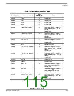
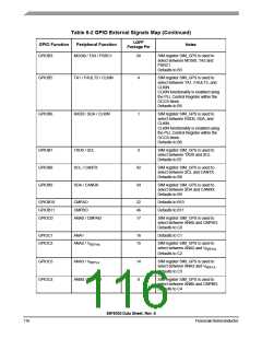
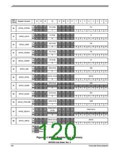
Table 8-2 GPIO External Signals Map (Continued)
LQFP
Package Pin
Notes
GPIO Function
Peripheral Function
GPIOB3
MOSI0 / TA3 / PSRC1
24
SIM register SIM_GPS is used to
select between MOSI0, TA3 and
PSRC1.
Defaults to B3
GPIOB5
GPIOB6
TA1 / FAULT3 / CLKIN
4
1
SIM register SIM_GPS is used to
select between TA1, FAULT3, and
CLKIN.
CLKIN functionality is enabled using
the PLL Control Register within the
OCCS block.
Defaults to B5
RXD0 / SDA / CLKIN
SIM register SIM_GPS is used to
select between RXD0, SDA, and
CLKIN.
CLKIN functionality is enabled using
the PLL Control Register within the
OCCS block.
Defaults to B6
GPIOB7
GPIOB8
GPIOB9
TXD0 / SCL
3
SIM register SIM_GPS is used to
select between TXD0 and SCL.
Defaults to B7
SCL / CANTX
SDA / CANRX
42
34
SIM register SIM_GPS is used to
select between SCL and CANTX.
Defaults to B8
SIM register SIM_GPS is used to
select between SDA and CANRX.
Defaults to B9
GPIOB10
GPIOB11
GPIOC0
CMPAO
22
46
17
Defaults to B10
Defaults to B11
CMPBO
ANA0 / CMPAI3
SIM register SIM_GPS is used to
select between ANA0 and CMPAI3.
Defaults to C0
GPIOC1
GPIOC2
ANA1
16
15
Defaults to C1
ANA2 / VREFHA
SIM register SIM_GPS is used to
select between ANA2 and VREFHA
.
Defaults to C2
GPIOC3
GPIOC4
ANA3 / VREFLA
ANB0 / CMPBI3
14
8
SIM register SIM_GPS is used to
select between ANA3 and VREFLA
.
Defaults to C3
SIM register SIM_GPS is used to
select between ANB0 and CMPBI3.
Defaults to C4
56F8036 Data Sheet, Rev. 6
116
FreescaleSemiconductor

 FREESCALE [ Freescale ]