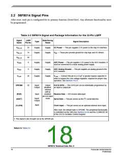
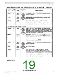
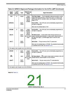
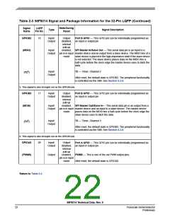
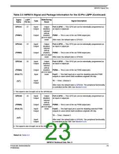
56F8014 Signal Pins
Table 2-3 56F8014 Signal and Package Information for the 32-Pin LQFP (Continued)
Signal
Name
LQFP
Pin No.
StateDuring
Reset
Type
Signal Description
GPIOB7
2
Input/
Output
Port B GPIO — This GPIO pin can be individually programmed as
Output
disabled, an input or output pin.
internal
pull-up
(TXD)
Input/
enabled,
Transmit Data — SCI transmit data output or transmit / receive in
Output
pin is in input single wire opeation.
mode
(SCL2)
Serial Clock — This pin serves as the I2C serial clock.
Input/
Output
After reset, the default state is GPIOB7. The peripheral functionality
is controlled via the SIM. See Section 6.3.8.
2. This signal is also brought out on the GPIOB0 pin.
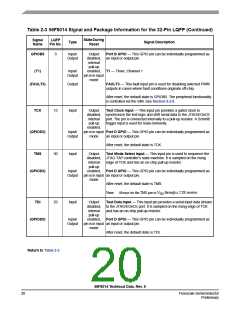
RESET
16
Input
Output
Reset — This input is a direct hardware reset on the processor.
disabled, When RESET is asserted low, the chip is initialized and placed in the
internal
pull-up
enabled,
pin is in input
mode
reset state. A Schmitt trigger input is used for noise immunity. The
internal reset signal will be deasserted synchronous with the internal
clocks after a fixed number of internal clocks.
(GPIOA7)
Input/Open
Drain
Port A GPIO — This GPIO pin can be individually programmed as
an input or open drain output pin. Note that RESET functionality is
disabled in this mode and the chip can only be reset via POR, COP
reset, or software reset.
Output
After reset, the default state is RESET.
GPIOB4
19
Input/
Output
Port B GPIO — This GPIO pin can be individually programmed as
Output
disabled, an input or output pin.
internal
pull-up
(T0)
Input/
Output
enabled,
pin is in input
mode
T0 — Timer, Channel 0
(CLKO)
Output
Clock Output — This is a buffered clock signal. Using the
SIM_CLKO Select Register (SIM_CLKOSR), this pin can be
programmed as any of the following: disabled (logic 0), CLK_MSTR
(system clock), IPBus clock, or oscillator output. See Section 6.3.7.
After reset, the default state is GPIOB4. The peripheral functionality
is controlled via the SIM. See Section 6.3.8.
Return to Table 2-2
56F8014 Technical Data, Rev. 9
Freescale Semiconductor
Preliminary
19

 FREESCALE [ Freescale ]