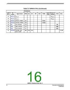
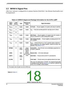
2.2 56F8014 Signal Pins
After reset, each pin is configured for its primary function (listed first). Any alternate functionality must
be programmed.
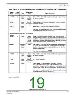
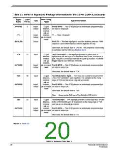
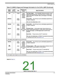
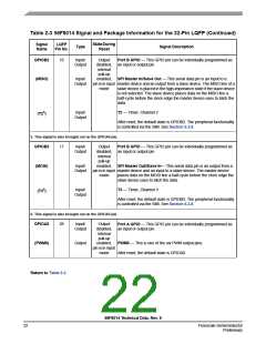
Table 2-3 56F8014 Signal and Package Information for the 32-Pin LQFP
Signal
Name
LQFP
Pin No.
StateDuring
Reset
Type
Signal Description
VDD_IO
VSS_IO
VSS_IO
VDDA
25
14
26
8
Supply
Supply
Supply
Supply
I/O Power — This pin supplies 3.3V power to the chip I/O interface.
VSS — These pins provide ground for chip logic and I/O drivers.
Supply
Supply
Supply
Supply
Supply
Supply
ADC Power — This pin supplies 3.3V power to the ADC modules. It
must be connected to a clean analog power supply.
VSSA
9
ADC Analog Ground — This pin supplies an analog ground to the
ADC modules.
VCAP
24
VCAP — Connect this pin to a 4.4μF or greater bypass capacitor in
order to bypass the core voltage regulator, required for proper chip
operation. See Section 10.2.1.
GPIOB6
32
Input/
Output
Port B GPIO — This GPIO pin can be individually programmed as
Output
disabled, an input or output pin.
internal
pull-up
(RXD)
Input
enabled,
pin is in input
mode
Receive Data — SCI receive data input.
(SDA1)
Serial Data — This pin serves as the I2C serial data line.
Input/
Output
Input
(CLKIN)
Clock Input — This pin serves as an optional external clock input.
After reset, the default state is GPIOB6. The peripheral functionality
is controlled via the SIM (See Section 6.3.8) and the CLKMODE bit
of the OCCS Oscillator Control Register.
1. This signal is also brought out on the GPIOB1 pin.
Return to Table 2-2
56F8014 Technical Data, Rev. 9
18
Freescale Semiconductor
Preliminary

 FREESCALE [ Freescale ]