FM25Q64ꢀ
ꢀ
11.ꢀCONTROLꢀANDꢀSTATUSꢀREGISTERꢀ
TheꢀReadꢀStatusꢀRegisterꢀinstructionꢀcanꢀbeꢀusedꢀtoꢀprovideꢀstatusꢀonꢀtheꢀavailabilityꢀofꢀtheꢀFlashꢀ
memoryꢀarray,ꢀifꢀtheꢀdeviceꢀisꢀwriteꢀenabledꢀorꢀdisabled,ꢀtheꢀstateꢀofꢀwriteꢀprotectionꢀandꢀtheꢀQuadꢀ
SPIꢀ setting.ꢀ Theꢀ Writeꢀ Statusꢀ Registerꢀ instructionꢀ canꢀ beꢀ usedꢀ toꢀ configureꢀ theꢀ devicesꢀ writeꢀ
protectionꢀfeaturesꢀandꢀQuadꢀSPIꢀsetting.ꢀWriteꢀaccessꢀtoꢀtheꢀStatusꢀRegisterꢀisꢀcontrolledꢀbyꢀinꢀ
someꢀcasesꢀofꢀtheꢀ/WPꢀpin.ꢀ
ꢀ
ꢀ
11.1ꢀSTATUSꢀREGISTERꢀ
ꢀ
11.1.1ꢀBUSYꢀ
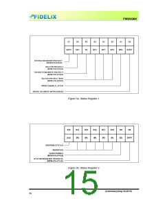
BUSYꢀ isꢀ aꢀ readꢀ onlyꢀ bitꢀ inꢀ theꢀ statusꢀ registerꢀ (S0)ꢀ thatꢀ isꢀ setꢀ toꢀ aꢀ 1ꢀ stateꢀ whenꢀ theꢀ deviceꢀ isꢀ
executingꢀ aꢀ Pageꢀ Program,ꢀ Sectorꢀ Erase,ꢀ Blockꢀ Erase,ꢀ Chipꢀ Eraseꢀ orꢀ Writeꢀ Statusꢀ Registerꢀ
instruction.ꢀDuringꢀthisꢀtimeꢀtheꢀdeviceꢀwillꢀignoreꢀfurtherꢀinstructionꢀexceptꢀforꢀtheꢀReadꢀStatusꢀ
Registerꢀ andꢀ Eraseꢀ Suspendꢀ instructionꢀ (seeꢀ tW,ꢀ tPP,ꢀ tSE,ꢀ tBE1,ꢀ tBE2ꢀ andꢀ tCEꢀ inꢀ ACꢀ
Characteristics).ꢀWhenꢀtheꢀprogram,ꢀeraseꢀorꢀwriteꢀstatusꢀregisterꢀinstructionꢀhasꢀcompleted,ꢀtheꢀ
BUSYꢀbitꢀwillꢀbeꢀclearedꢀtoꢀaꢀ0ꢀstateꢀindicatingꢀtheꢀdeviceꢀisꢀreadyꢀforꢀfurtherꢀinstructions.ꢀ
ꢀ
ꢀ
11.1.2ꢀWriteꢀEnableꢀLatchꢀ(WEL)ꢀ
Writeꢀ Enableꢀ Latchꢀ (WEL)ꢀ isꢀ aꢀ readꢀ onlyꢀ bitꢀ inꢀ theꢀ statusꢀ registerꢀ (S1)ꢀ thatꢀ isꢀ setꢀ toꢀ aꢀ 1ꢀ afterꢀ
executingꢀaꢀWriteꢀEnableꢀinstruction.ꢀTheꢀWELꢀstatusꢀbitꢀisꢀclearedꢀtoꢀaꢀ0,ꢀWhenꢀdeviceꢀisꢀwriteꢀ
disabled.ꢀ ꢀ Aꢀwriteꢀdisableꢀstateꢀoccursꢀuponꢀpowerꢁupꢀorꢀafterꢀanyꢀofꢀtheꢀfollowingꢀinstructions:ꢀ
WriteꢀDisable,ꢀPageꢀProgram,ꢀSectorꢀErase,ꢀBlockꢀErase,ꢀChipꢀEraseꢀandꢀWriteꢀStatusꢀRegister.ꢀ
ꢀ
ꢀ
11.1.3ꢀBlockꢀProtectꢀBitsꢀ(BP2,ꢀBP1,ꢀBP0)ꢀ
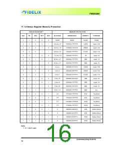
TheꢀBlockꢀProtectꢀBitsꢀ(BP2,ꢀBP1,ꢀBP0)ꢀareꢀnonꢁvolatileꢀread/writeꢀbitsꢀinꢀtheꢀstatusꢀregisterꢀ(S4,ꢀ
S3,ꢀandꢀS2)ꢀthatꢀprovideꢀwriteꢀprotectionꢀcontrolꢀandꢀstatus.ꢀBlockꢀprotectꢀbitsꢀcanꢀbeꢀsetꢀusingꢀtheꢀ
WriteꢀStatusꢀRegisterꢀInstructionꢀ(seeꢀtWꢀinꢀACꢀcharacteristics).ꢀAllꢀnoneꢀorꢀaꢀportionꢀofꢀtheꢀmemoryꢀ
arrayꢀ canꢀ beꢀ protectedꢀ fromꢀ Programꢀ andꢀ Eraseꢀ instructionsꢀ (seeꢀ Statusꢀ Registerꢀ Memoryꢀ
Protectionꢀtable).ꢀTheꢀfactoryꢀdefaultꢀsettingꢀforꢀtheꢀBlockꢀProtectionꢀBitsꢀisꢀ0,ꢀnoneꢀofꢀtheꢀarrayꢀ
protected.ꢀ
ꢀ
ꢀ
11.1.4ꢀTop/BottomꢀBlockꢀprotectꢀ(TB)ꢀ
TheꢀnonꢁvolatileꢀTop/Bottomꢀbitꢀ(TB)ꢀcontrolsꢀifꢀtheꢀBlockꢀProtectꢀBitsꢀ(BP2,ꢀBP1,ꢀBP0)ꢀprotectꢀfromꢀ
theꢀ Topꢀ (TB=0)ꢀ orꢀ theꢀ Bottomꢀ (TB=1)ꢀ ofꢀ theꢀ arrayꢀ asꢀ shownꢀ inꢀ theꢀ Statusꢀ Registerꢀ Memoryꢀ
Protectionꢀtable.ꢀTheꢀfactoryꢀdefaultꢀsettingꢀisꢀTB=0.ꢀTheꢀTBꢀbitꢀcanꢀbeꢀsetꢀwithꢀtheꢀWriteꢀStatusꢀ
RegisterꢀInstructionꢀdependingꢀonꢀtheꢀstateꢀofꢀtheꢀSRP0,ꢀSRP1ꢀandꢀWELꢀbits.ꢀ
ꢀ
ꢀ
11.1.5ꢀSector/BlockꢀProtectꢀ(SEC)ꢀ
TheꢀnonꢁvolatileꢀSectorꢀprotectꢀbitꢀ(SEC)ꢀcontrolsꢀifꢀtheꢀBlockꢀProtectꢀBitsꢀ(BP2,ꢀBP1,ꢀBP0)ꢀprotectꢀ
4KBꢀSectorsꢀ(SEC=1)orꢀ64KBꢀBlocksꢀ(SEC=0)ꢀinꢀtheꢀTopꢀ(TB=0)ꢀorꢀtheꢀBottomꢀ(TB=1)ꢀofꢀtheꢀarrayꢀ
asꢀshownꢀinꢀtheꢀStatusꢀRegisterꢀMemoryꢀprotectionꢀtable.ꢀTheꢀdefaultꢀsettingꢀisꢀSEC=0.ꢀ
preliminary(Aug.18.2010)ꢀ ꢀ ꢀ ꢀ
13ꢀ

 FIDELIX [ FIDELIX ]