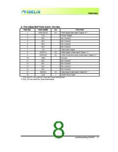
FM25Q64ꢀ
ꢀ
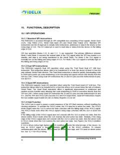
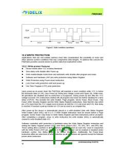
ꢀ ꢀ ꢀ ꢀ ꢀ ꢀ ꢀ ꢀ ꢀ ꢀ ꢀ ꢀ ꢀ ꢀ ꢀ ꢀ ꢀ ꢀ ꢀ ꢀ ꢀ ꢀ Figure2.ꢀHoldꢀconditionꢀwaveformꢀ
ꢀ
ꢀ
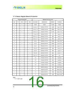
10.2ꢀWRITEꢀPROTECTIONꢀ
Applicationsꢀ thatꢀ useꢀ nonꢁvolatileꢀ memoryꢀ mustꢀ takeꢀ considerationꢀ theꢀ possibilityꢀ ofꢀ noiseꢀ andꢀ
otherꢀadverseꢀsystemꢀconditionsꢀthatꢀmayꢀcompromiseꢀdataꢀintegrity.ꢀToꢀaddressꢀthisꢀconcernꢀtheꢀ
FM25Q64ꢀprovidesꢀseveralꢀmeansꢀtoꢀprotectꢀdataꢀfromꢀinadvertentꢀwrites.ꢀ
ꢀ
10.2.1ꢀWriteꢀprotectꢀFeaturesꢀ
ꢀꢀ DeviceꢀresetsꢀwhenꢀVCCꢀisꢀbelowꢀthresholdꢀ
ꢀꢀ TimeꢀdelayꢀwriteꢀdisableꢀafterꢀPowerꢁupꢀ
ꢀꢀ Writeꢀenable/disableꢀinstructionsꢀandꢀautomaticꢀwriteꢀdisableꢀafterꢀprogramꢀandꢀeraseꢀ
ꢀꢀ SoftwareꢀandꢀHardwareꢀ(/WPꢀpin)ꢀwriteꢀprotectionꢀusingꢀStatusꢀRegisterꢀ
ꢀꢀ WriteꢀProtectionꢀusingꢀPowerꢁdownꢀinstructionꢀ
ꢀꢀ LockꢀDownꢀwriteꢀprotectionꢀuntilꢀnextꢀpowerꢁupꢀ
ꢀꢀ OneꢀTimeꢀProgramꢀ(OTP)ꢀwriteꢀprotectionꢀ
ꢀ
UponꢀpowerꢁupꢀatꢀpowerꢀdownꢀtheꢀFM25Q64ꢀwillꢀmaintainꢀaꢀresetꢀconditionꢀwhileꢀVCCꢀisꢀbelowꢀ
theꢀthresholdꢀvalueꢀofꢀVWI,ꢀ(SeeꢀPowerꢁupꢀTimingꢀandꢀVoltageꢀLevelsꢀandꢀFigureꢀ30).ꢀWhileꢀreset,ꢀ
allꢀoperationsꢀareꢀdisabledꢀandꢀnoꢀinstructionꢀisꢀrecognized.ꢀDuringꢀpowerꢁupꢀandꢀafterꢀtheꢀVCCꢀ
voltageꢀexceedsꢀVWI,ꢀinstructionsꢀrelatedꢀwithꢀallꢀprogramꢀandꢀeraseꢀareꢀfurtherꢀdisabledꢀforꢀaꢀtimeꢀ
delayꢀofꢀtPUW.ꢀThisꢀincludesꢀtheꢀwriteꢀEnable,ꢀPageꢀprogram,ꢀSectorꢀErase,ꢀBlockꢀErase,ꢀChipꢀ
Erase,ꢀWriteꢀSecurityꢀRegisterꢀandꢀtheꢀWriteꢀStatusꢀRegisterꢀinstructions.ꢀNoteꢀthatꢀtheꢀchipꢀselectꢀ
pinꢀ(/CS)ꢀmustꢀtrackꢀtheꢀVCCꢀsupplyꢀlevelꢀatꢀpowerꢁupꢀuntilꢀtheꢀVCCꢁminꢀlevelꢀandꢀtVSLꢀtimeꢀdelayꢀ
isꢀreached.ꢀIfꢀneededꢀaꢀpullꢁupꢀresisterꢀonꢀ/CSꢀcanꢀbeꢀusedꢀtoꢀaccomplishꢀthis.ꢀ
ꢀ
Afterꢀ powerꢁupꢀ theꢀ deviceꢀ isꢀ automaticallyꢀ placedꢀ inꢀ aꢀ writeꢁdisabledꢀ stateꢀ withꢀ Statusꢀ Registerꢀ
WriteꢀEnableꢀLatchꢀ(WEL)ꢀsetꢀtoꢀaꢀ0.ꢀAꢀWriteꢀEnableꢀinstructionꢀmustꢀbeꢀissuedꢀbeforeꢀaꢀPageꢀ
program,ꢀSectorꢀEraseꢀChipꢀEraseꢀorꢀWriteꢀStatusꢀRegisterꢀandꢀthenꢀinstructionsꢀwillꢀbeꢀaccepted.ꢀ
Afterꢀ completingꢀ aꢀ program,ꢀ eraseꢀ orꢀ writeꢀ instructionꢀ theꢀ writeꢀ Enableꢀ (WEL)ꢀ isꢀ automaticallyꢀ
clearedꢀtoꢀwriteꢁdisabledꢀstateꢀofꢀ0.ꢀ
ꢀ
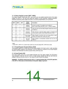
Softwareꢀ controlledꢀ writeꢀ protectionꢀ isꢀ facilitatedꢀusingꢀ theꢀWriteꢀ Statusꢀ Registerꢀ instructionꢀ andꢀ
settingꢀtheꢀStatusꢀRegisterꢀprotectꢀ(SRP)ꢀandꢀBlockꢀprotectꢀ(SEC,ꢀTB,ꢀBP2,ꢀBP1,ꢀandꢀBP0)ꢀbits.ꢀ
Theseꢀsettingꢀallowꢀaꢀportionꢀorꢀallꢀtheꢀmemoryꢀtoꢀbeꢀconfiguredꢀasꢀreadꢀonly.ꢀUsedꢀinꢀconjunctionꢀ
withꢀtheꢀWriteꢀProtectꢀ(/WP)ꢀpin,ꢀchangesꢀtoꢀtheꢀStatusꢀRegisterꢀcanꢀbeꢀenabledꢀorꢀdisabledꢀunderꢀ
hardwareꢀ control.ꢀ Seeꢀ Statusꢀ Registerꢀ forꢀ furtherꢀ information.ꢀ Additionally,ꢀ theꢀ Powerꢁdownꢀ
instructionꢀoffersꢀanꢀextraꢀlevelꢀofꢀwriteꢀprotectionꢀasꢀallꢀinstructionsꢀareꢀignoredꢀexceptꢀforꢀReleaseꢀ
powerꢁdownꢀinstruction.ꢀ
preliminary(Aug.18.2010)ꢀ ꢀ ꢀ ꢀ
12ꢀ

 FIDELIX [ FIDELIX ]