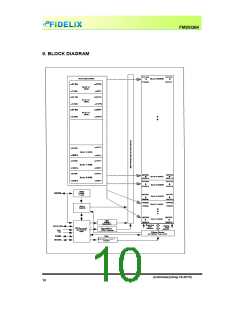
FM25Q64ꢀ
ꢀ
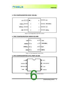
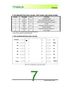
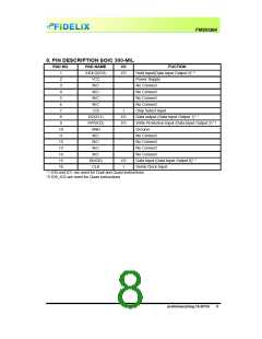
8.1ꢀPackageꢀTypesꢀ
8ꢁpinꢀ plasticꢀ 208ꢁmilꢀ widthꢀ SOIC,ꢀ 6x5ꢁmmꢀ WSON,ꢀ 8ꢁpinꢀ PDIPꢀ andꢀ 16ꢁpinꢀ plasticꢀ 300ꢁmilꢀ widthꢀ
SOICꢀasꢀshownꢀinꢀfigureꢀ1a,ꢀ1b,1cꢀandꢀ1dꢀrespectively.ꢀ ꢀ
Packageꢀdiagramsꢀandꢀdimensionsꢀareꢀillustratedꢀatꢀtheꢀendꢀofꢀthisꢀdatasheet.ꢀ
ꢀ
8.2ꢀChipꢀSelectꢀ(/CS)ꢀ
TheꢀSPIꢀChipꢀSelectꢀ(/CS)ꢀpinꢀenablesꢀandꢀdisablesꢀdeviceꢀoperation.ꢀWhenꢀ/CSꢀisꢀhighꢀtheꢀdeviceꢀ
isꢀdeselectedꢀandꢀtheꢀSerialꢀDataꢀOutputꢀ(DO,ꢀorꢀIO0,ꢀIO1,ꢀIO2,ꢀIO3)ꢀpinsꢀareꢀatꢀhighꢀimpedance.ꢀ
Whenꢀdeselected,ꢀtheꢀdeviceꢀpowerꢀconsumptionꢀwillꢀbeꢀatꢀstandbyꢀlevelsꢀunlessꢀanꢀinternalꢀerase,ꢀ
programꢀorꢀwriteꢀstatusꢀregisterꢀcycleꢀisꢀinꢀprogress.ꢀWhenꢀ/CSꢀisꢀbroughtꢀlowꢀtheꢀdeviceꢀwillꢀbeꢀ
selected,ꢀpowerꢀconsumptionꢀwillꢀincreaseꢀtoꢀactiveꢀlevelsꢀandꢀinstructionsꢀcanꢀbeꢀwrittenꢀtoꢀandꢀ
readꢀ dataꢀ fromꢀ theꢀ device.ꢀ Afterꢀ powerꢁup,ꢀ /CSꢀ mustꢀ transitionꢀ fromꢀ highꢀ toꢀ lowꢀ beforeꢀ aꢀ newꢀ
instructionꢀwillꢀbeꢀaccepted.ꢀTheꢀ/CSꢀinputꢀmustꢀtrackꢀtheꢀVCCꢀsupplyꢀlevelꢀatꢀpowerꢁupꢀ(seeꢀ“Writeꢀ
Protection”ꢀandꢀfigureꢀ30).ꢀIfꢀneededꢀaꢀpullꢁupꢀresisterꢀonꢀ/CSꢀcanꢀbeꢀusedꢀtoꢀaccomplishꢀthis.ꢀ
ꢀ
8.3ꢀSerialꢀDataꢀInput,ꢀOutputꢀandꢀIOsꢀ(DI,ꢀDOꢀandꢀIO0,ꢀIO1,ꢀIO2,ꢀIO3)ꢀ
Theꢀ FM25Q64ꢀ supportsꢀ standardꢀ SPI,ꢀ Dualꢀ SPIꢀ andꢀ Quadꢀ SPIꢀ operation.ꢀ Standardꢀ SPIꢀ
instructionsꢀuseꢀtheꢀunidirectionalꢀDIꢀ(input)ꢀpinꢀtoꢀseriallyꢀwriteꢀinstructions,ꢀaddressesꢀorꢀdataꢀtoꢀ
theꢀ deviceꢀ onꢀ theꢀ risingꢀ edgeꢀ ofꢀ theꢀ Serialꢀ Clockꢀ (CLK)ꢀ inputꢀ pin.ꢀ Standardꢀ SPIꢀ alsoꢀ usesꢀ theꢀ
unidirectionalꢀDOꢀ(output)ꢀtoꢀreadꢀdataꢀorꢀstatusꢀfromꢀtheꢀdeviceꢀonꢀtheꢀfallingꢀedgeꢀofꢀCLK.ꢀ
ꢀ
Dualꢀ andꢀ Quadꢀ SPIꢀ instructionsꢀ useꢀ theꢀ bidirectionalꢀ IOꢀ pinsꢀ toꢀ seriallyꢀ writeꢀ instructions,ꢀ
addressesꢀorꢀdataꢀtoꢀtheꢀdeviceꢀonꢀtheꢀrisingꢀedgeꢀofꢀCLKꢀandꢀreadꢀdataꢀorꢀstatusꢀfromꢀtheꢀdeviceꢀ
onꢀtheꢀfallingꢀedgeꢀofꢀCLK.ꢀQuadꢀSPIꢀinstructionsꢀrequireꢀtheꢀnonꢁvolatileꢀQuadꢀEnableꢀbitꢀ(QE)ꢀinꢀ
StatusꢀRegisterꢁ2ꢀtoꢀbeꢀset.ꢀWhenꢀQE=1ꢀtheꢀ/WPꢀpinꢀbecomesꢀIO2ꢀandꢀ/HOLDꢀpinꢀbecomesꢀIO3.ꢀ
ꢀ
8.4ꢀWriteꢀProtectꢀ(/WP)ꢀ
TheꢀWriteꢀProtectꢀ(/WP)ꢀpinꢀcanꢀbeꢀusedꢀtoꢀpreventꢀtheꢀStatusꢀRegisterꢀfromꢀbeingꢀwritten.ꢀUsedꢀinꢀ
conjunctionꢀwithꢀtheꢀStatusꢀRegister’sꢀBlockꢀProtectꢀ(SEC.ꢀTB.ꢀBP2,ꢀBp1ꢀandꢀBP0)ꢀbitsꢀandꢀStatusꢀ ꢀ
RegisterꢀProtectꢀ(SRP)ꢀbits,ꢀaꢀportionꢀorꢀtheꢀentireꢀmemoryꢀarrayꢀcanꢀbeꢀhardwareꢀprotected.ꢀTheꢀ
/WPꢀ pinꢀ isꢀ activeꢀ low.ꢀ Whenꢀ theꢀ QEꢀ bitꢀ ofꢀ Statusꢀ Registerꢁ2ꢀ isꢀ setꢀ forꢀ Quadꢀ I/O,ꢀ theꢀ /WPꢀ pinꢀ
(HardwareꢀWriteꢀProtect)ꢀfunctionꢀisꢀnotꢀavailableꢀsinceꢀthisꢀpinꢀisꢀusedꢀforꢀIO2.ꢀSeeꢀfigureꢀ1a,ꢀ1b,ꢀ
1cꢀandꢀ1dꢀforꢀtheꢀpinꢀconfigurationꢀofꢀQuadꢀI/Oꢀoperation.ꢀ
ꢀ
8.5ꢀHOLDꢀ(/HOLD)ꢀ
Theꢀ/HOLDꢀpinꢀallowsꢀtheꢀdeviceꢀtoꢀbeꢀpausedꢀwhileꢀitꢀisꢀactivelyꢀselected.ꢀWhenꢀ/HOLDꢀisꢀbroughtꢀ
low,ꢀwhileꢀ/CSꢀisꢀlow,ꢀtheꢀDOꢀpinꢀwillꢀbeꢀatꢀhighꢀimpedanceꢀandꢀsignalsꢀonꢀtheꢀDIꢀandꢀCLKꢀpinsꢀwillꢀ
beꢀignoredꢀ(don’tꢀcare).ꢀWhenꢀ/HOLDꢀisꢀbroughtꢀhigh,ꢀdeviceꢀoperationꢀcanꢀresume.ꢀTheꢀ/HOLDꢀ
functionꢀcabꢀbeꢀusefulꢀwhenꢀmultipleꢀdevicesꢀareꢀsharingꢀtheꢀsameꢀSPIꢀsignals.ꢀTheꢀ/HOLDꢀpinꢀisꢀ
activeꢀlow.ꢀWhenꢀtheꢀQEꢀbitꢀofꢀStatusꢀRegisterꢁ2ꢀisꢀsetꢀQuadꢀI/O,ꢀtheꢀ/HOLDꢀpinꢀfunctionꢀisꢀnotꢀ
availableꢀsinceꢀthisꢀpinꢀusedꢀforꢀIO3.ꢀSeeꢀfigureꢀ1a,ꢀ1b,ꢀ1cꢀandꢀ1dꢀforꢀtheꢀpinꢀconfigurationꢀofꢀQuadꢀ
I/Oꢀoperation.ꢀ
ꢀ ꢀ ꢀ ꢀ ꢀ ꢀ ꢀ ꢀ ꢀ ꢀ ꢀ ꢀ ꢀ ꢀ ꢀ ꢀ ꢀ ꢀ ꢀ ꢀ ꢀ ꢀ ꢀ ꢀ ꢀ
8.6ꢀSerialꢀClockꢀ(CLK)ꢀ
TheꢀSPIꢀSerialꢀClockꢀInputꢀ(CLK)ꢀpinꢀprovidesꢀtheꢀtimingꢀforꢀserialꢀinputꢀandꢀoutputꢀoperations.ꢀ
(“SeeꢀSPIꢀOperations”)ꢀ
ꢀ
ꢀ
ꢀ
ꢀ
ꢀ
preliminary(Aug.18.2010)ꢀ ꢀ ꢀ ꢀ 9ꢀ

 FIDELIX [ FIDELIX ]