FM25Q64ꢀ
ꢀ
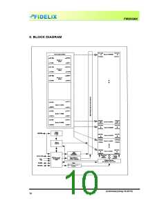
10.ꢀ ꢀ FUNCTIONALꢀDESCRIPTIONꢀ
ꢀ
10.1ꢀSPIꢀOPERATIONSꢀ
ꢀ
10.1.1ꢀStandardꢀSPIꢀInstructionsꢀ
TheꢀFM25Q64ꢀisꢀaccessedꢀthroughꢀanꢀSPIꢀcompatibleꢀbusꢀconsistingꢀofꢀfourꢀsignals:ꢀSerialꢀClockꢀ
(CLK).ꢀ Chipꢀ Selectꢀ (/CS),ꢀ Serialꢀ Dataꢀ Inputꢀ (DI)ꢀ andꢀ Serialꢀ Dataꢀ Outputꢀ (DO).ꢀ Standardꢀ SPIꢀ
instructionsꢀuseꢀtheꢀDIꢀinputꢀpinꢀtoꢀseriallyꢀwriteꢀinstructions,ꢀaddressesꢀorꢀdataꢀtoꢀtheꢀdeviceꢀonꢀtheꢀ
risingꢀedgeꢀofꢀCLK.ꢀTheꢀDOꢀoutputꢀpinꢀisꢀusedꢀtoꢀreadꢀdataꢀorꢀstatusꢀfromꢀtheꢀdeviceꢀonꢀtheꢀfallingꢀ
edgeꢀofꢀCLK.ꢀ
ꢀ
SPIꢀ busꢀ operationꢀ Modesꢀ 0ꢀ (0,ꢀ 0)ꢀ andꢀ 3ꢀ (1,ꢀ 1)ꢀ areꢀsupported.ꢀ Theꢀ primaryꢀ differenceꢀ betweenꢀ
Modeꢀ0ꢀandꢀModeꢀ3ꢀconcernsꢀtheꢀnormalꢀstateꢀofꢀtheꢀCLKꢀsignalꢀwhenꢀtheꢀSPIꢀbusꢀmasterꢀisꢀinꢀ
standbyꢀ andꢀ dataꢀ isꢀ notꢀ beingꢀ transferredꢀ toꢀ theꢀ Serialꢀ Flash.ꢀ Forꢀ Modeꢀ 0ꢀ theꢀ CLKꢀ signalꢀ isꢀ
normallyꢀlowꢀonꢀtheꢀfallingꢀandꢀrisingꢀedgesꢀofꢀ/CS.ꢀForꢀModeꢀ3ꢀtheꢀCLKꢀsignalꢀisꢀnormallyꢀhighꢀonꢀ
theꢀfallingꢀandꢀrisingꢀedgesꢀofꢀ/CS.ꢀ
ꢀ
10.1.2ꢀDualꢀSPIꢀInstructionsꢀ
Theꢀ FM25Q64ꢀ supportsꢀ Dualꢀ SPIꢀ operationꢀ whenꢀ usingꢀ theꢀ “Fastꢀ Readꢀ Dualꢀ I/O”ꢀ (BBꢀ hex)ꢀ
instruction.ꢀThisꢀinstructionꢀallowsꢀdataꢀtoꢀbeꢀtransferredꢀtoꢀorꢀfromꢀtheꢀdeviceꢀatꢀthreeꢀtoꢀfourꢀtheꢀ
rateꢀordinaryꢀSerialꢀFlashꢀdevices.ꢀTheꢀDualꢀReadꢀinstructionꢀisꢀidealꢀforꢀquicklyꢀdownloadingꢀcodeꢀ
toꢀRAMꢀuponꢀpowerꢁupꢀ(codeꢁshadowing)ꢀorꢀforꢀexecutingꢀnonꢁspeedꢁcriticalꢀcodeꢀdirectlyꢀfromꢀtheꢀ
SPIꢀbusꢀ(XIP).ꢀWhenꢀusingꢀDualꢀSPIꢀinstructionsꢀtheꢀDIꢀandꢀDOꢀpinsꢀbecomeꢀbidirectionalꢀI/0ꢀpins;ꢀ
IO0ꢀandꢀIO1.ꢀ
ꢀ
10.1.3ꢀQuadꢀSPIꢀInstructionsꢀ
TheꢀFM25Q64ꢀsupportsꢀQuadꢀSPIꢀoperationꢀwhenꢀusingꢀtheꢀ“FastꢀReadꢀQuadꢀI/O”ꢀ(EBꢀhex).ꢀThisꢀ
instructionꢀallowsꢀdataꢀtoꢀbeꢀtransferredꢀtoꢀorꢀfromꢀtheꢀdeviceꢀsixꢀtoꢀsevenꢀtimesꢀtheꢀrateꢀofꢀordinaryꢀ
Serialꢀ Flash.ꢀ Theꢀ Quadꢀ Readꢀ instructionꢀ offersꢀ aꢀ significantꢀ improvementꢀ inꢀ continuousꢀ andꢀ
randomꢀaccessꢀtransferꢀratesꢀallowingꢀfastꢀcodeꢁshadowingꢀtoꢀRAMꢀorꢀexecutionꢀdirectlyꢀfromꢀtheꢀ
SPIꢀbusꢀ(XIP).ꢀWhenꢀusingꢀQuadꢀSPIꢀinstructionꢀtheꢀDIꢀandꢀDOꢀpinsꢀbecomeꢀbidirectionalꢀIO0ꢀandꢀ
IO1,ꢀandꢀtheꢀ/WPꢀandꢀ/HOLDꢀpinsꢀbecomeꢀIO2ꢀandꢀIO3ꢀrespectively.ꢀQuadꢀSPIꢀinstructionsꢀrequireꢀ
theꢀnonꢁvolatileꢀQuadꢀEnableꢀbitꢀ(QE)ꢀinꢀStatusꢀRegisterꢁ2ꢀtoꢀbeꢀset.ꢀ
ꢀ
10.1.4ꢀHoldꢀFunctionꢀ
Theꢀ/HOLDꢀpinꢀisꢀusedꢀtoꢀpauseꢀaꢀserialꢀsequenceꢀofꢀtheꢀSPIꢀflashꢀmemoryꢀwithoutꢀresettingꢀtheꢀ
clockingꢀsequence.ꢀToꢀactivateꢀtheꢀ/HOLDꢀmode,ꢀtheꢀ/CSꢀmustꢀbeꢀinꢀactiveꢀlowꢀstate.ꢀTheꢀ/HOLDꢀ
modeꢀbeginsꢀwhenꢀtheꢀCLKꢀinꢀactiveꢀlowꢀstateꢀcoincidesꢀwithꢀtheꢀfallingꢀedgeꢀofꢀtheꢀ/HOLDꢀsignal.ꢀ
TheꢀHOLDꢀmodeꢀendsꢀwhenꢀtheꢀ/HOLDꢀsignal’sꢀrisingꢀedgeꢀcoincidesꢀwithꢀtheꢀCLKꢀinꢀactiveꢀlowꢀ
state.ꢀ
Ifꢀtheꢀfallingꢀedgeꢀofꢀtheꢀ/HOLDꢀsignalꢀdoesꢀnotꢀcoincideꢀwithꢀtheꢀCLKꢀinꢀactiveꢀlowꢀstate,ꢀthenꢀtheꢀ
deviceꢀentersꢀHOLDꢀmodeꢀwhenꢀtheꢀCLKꢀreachesꢀtheꢀnextꢀactiveꢀlowꢀstate.ꢀSimilarly,ꢀifꢀtheꢀrisingꢀ
edgeꢀofꢀtheꢀ/HOLDꢀsignalꢀdoesꢀnotꢀcoincideꢀwithꢀtheꢀCLKꢀinꢀactiveꢀlowꢀstate,ꢀthenꢀtheꢀdeviceꢀexitsꢀ
inꢀHOLDꢀmodeꢀwhenꢀtheꢀCLKꢀreachesꢀtheꢀnextꢀactiveꢀlowꢀstate.ꢀSeeꢀFigure.2ꢀforꢀHOLDꢀconditionꢀ
waveform.ꢀ
Ifꢀ/CSꢀisꢀdrivenꢀactiveꢀhighꢀduringꢀaꢀHOLDꢀcondition,ꢀitꢀresetsꢀtheꢀinternalꢀlogicꢀofꢀtheꢀdevice.ꢀAsꢀ
longꢀ asꢀ /HOLDꢀ signalꢀ isꢀ low,ꢀ theꢀ memoryꢀ remainsꢀ inꢀ theꢀ HOLDꢀ condition.ꢀ Toꢀ resumeꢀ
communicationꢀwithꢀtheꢀdevice,ꢀ/HOLDꢀmustꢀbeꢀdrivenꢀactiveꢀhigh,ꢀandꢀ/CSꢀmustꢀbeꢀdrivenꢀactiveꢀ
low.ꢀSeeꢀ12.11ꢀforꢀHOLDꢀtiming.ꢀ
ꢀ
preliminary(Aug.18.2010)ꢀ ꢀ ꢀ ꢀ
11ꢀ

 FIDELIX [ FIDELIX ]