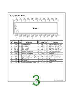
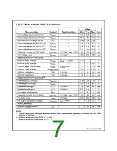
ELECTRICAL CHARACTERISTICS
5.
(continued)
Value
Characteristic
Symbol
VOVP2
VOVP3
VPT
Test Condition
Min. Typ. Max. Unit
Over voltage protection for 5V
Over voltage protection for 12V
Input threshold voltage for PT
Under voltage protection for 3.3V
Under voltage protection for 5V
Under voltage protection for 12V
Charging current for UVP delay
UVP Delay Time
–
–
–
–
–
–
5.8 6.2 6.6
13.5 14.2 15.0
1.20 1.25 1.30
2.1 2.3 2.5
3.7 4.0 4.3
V
V
VUVP1
VUVP2
VUVP3
ICHG.UVP
TD.UVP
V
V
9.2
10 10.8
V
C=2.2µF, VTH =1.8V -10 -15 -23
uA
C=2.2µF
100 260 500 ms
REMOTE ON/OFF SECTION
REM on input voltage
VREMH
VREML
IREML
IREM = -200µA
–
2.0
–
–
–
–
V
V
REM off input voltage
0.8
REM off input bias voltage
REM on open voltage
VREM =0.4V
–
–
–
-1.6 mA
VREM(OPEN)
Ton
2.0
4
–
5.25
14
V
REM on delay time
C=0.1µF
C=0.1µF
8
ms
ms
REM off delay time
Toff
16
24
34
REMOTE ON/OFF SECTION(2)
Detecting input voltage
Detecting V5 voltage
VIN(DET)
V5(DET)
HY1
–
1.20 1.25 1.30
4.1 4.3 4.5
V
V
–
COMP1, 2
COMP3
–
Hysteresis voltage 1
10
0.6 1.2
0.5
40
80
–
mV
V
Hysteresis voltage 2
HY2
Ω
k
PG output load resistor
Charging current for PG delay
PG delay time
RPG
1
2
ICHG.PG
TD.PG
C=2.2µF, VTH =1.8V -10 -15 -23
uA
C=2.2µF
100 260 500 ms
PG output saturation voltage
TOTAL DEVICE
VSAT(PG)
IPG =10mA
–
–
0.4 0.2
V
Standby supply current
ICC
–
10
20
mA
Notes:
1. These Parameters, although guaranteed over their recommended operating conditions are not 100%
tested in production.
2. REM on delay time (Pin6 REM: “L” → “H”),
REM off delay time (Pin6 REM: “H” → “L”)
Rev C, November 1999
7

 FAIRCHILD [ FAIRCHILD SEMICONDUCTOR ]