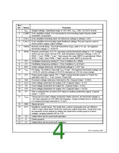
Pin
No. Name
Function
Supply voltage. Operating range is 14V~30V. VCC =20V, Ta=25 C at test.
°
1
2
VCC
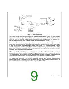
COMP Error amplifier output. It is connected to non-inverting input of pulse width
modulator comparator.
3
4
E/A(-) Error amplifier inverting input. Its reference voltage is always 1.25V.
E/A(+) Error amplifier non-inverting input feedback voltage.This pin may be used to
sense power supply output voltage.
5
6
TREM Remote on/off delay. Ton/Toff=8ms/24ms (Typ.) with C=0.1µF. Its high/low
threshold voltage is 1.8V/0.6V.
REM
Remote on/off input. It is TTL operation and its threshold voltage is 1.4V. Voltage
at this pin can reach normal 4.6V, with absolutely maximum voltage, 5.25V. If
REM = “Low”, PWM = “Low”. That means the main SMPS is operational. When
REM = “High”, then PWM = “High” and the main SMPS is turned-off.
Ω
7
8
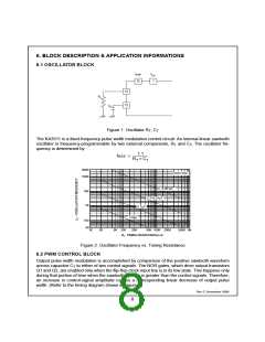
RT
CT
Oscillation frequency setting R. (Test Condition RT=10k )
Oscillation frequency setting C. (Test Condition CT=0.01µF)
Under-voltage detect pin. Its threshold voltage is 1.25V Typ.
9
DET
TPG
10
PG delay. Td=250ms (Typ) with CPG=2.2µF. The high/low threshold voltage are
1.8V/0.6V and the voltage of Pin10 is clamped at 2.9V for noise margin.
11
PG
Power good output signal. PG = “High” means that the power is “Good” for
operation and PG = “Low” means “Power fail”.
12
13
14
15
16
Vref
V3.3
V5
Precision voltage reference trimmed to 2%. (Typical Value = 5.03V)
Over voltage protection for output 3.3V. (Typical Value = 4.1V)
Over voltage protection for output 5V. (Typical Value = 6.2V)
Over voltage protection for output 12V. (Typical Value = 14.2V)
V12
PT
This is prepared for an extra OVP input or another protection signal. (Typical
Value = 1.25V)
17
TUVP
Timing pin for under voltage protection blank-out time. Its threshold voltage is
1.8V and clamped at 2.9V after full charging. Target of delay time is 250ms and
it is realized through external (C=2.2µF).
18
19
GND
DTC
Signal ground.
Deadtime control input. The dead-time control comparator has an effective
120mV input offset which limits the minimum output dead time. Dead time may
be imposed on the output by setting the dead time control input to a fixed
voltage, ranging between 0V to 3.3V.
20
21
22
C2
E
Output drive pin for push-pull operation.
Power ground.
C1
Output drive pin for push-pull operation.
Rev C, November 1999
4

 FAIRCHILD [ FAIRCHILD SEMICONDUCTOR ]