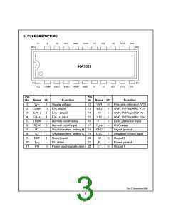
3. PIN DESCRIPTION
C1
E
C2
DTC
GND
TUVP
PT
V12
V5
V3.3
Vref
#22
#12
KA3511
#1
#11
VCC
COMPE/A(-)
EA(+)
TREM
REM
RT
CT
DET
GTP G P
Pin
No. Name I/O
Pin
Function
Supply voltage
No. Name I/O
Function
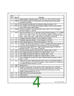
1
2
VCC
COMP
E/A(-)
E/A(+)
TREM
REM
RT
I
O
I
12
13
14
15
16
17
Vref
V3.3
V5
O
I
Precision reference VTG
OVP, UVP input for 3.3V
OVP, UVP input for 5V
OVP, UVP input for 12V
Extra protection input
UVP delay
E/A output
3
E/A (-) input
I
4
I
E/A (+) input
V12
PT
I
5
–
I
Remote on/off delay
Remote on/off input
I
6
TUVP
GND
DTC
C2
–
–
I
7
–
–
I
Oscillation freq. setting R 18
Oscillation freq. setting C 19
Signal ground
8
CT
Deadtime control input
Output 2
9
DET
TPG
Detect input
PG delay
20
21
O
–
O
10
11
–
O
E
Power ground
PG
Power good signal output 22
C1
Output 1
Rev C, November 1999
3

 FAIRCHILD [ FAIRCHILD SEMICONDUCTOR ]