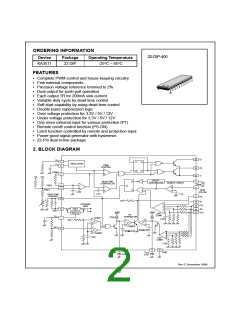
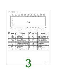
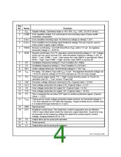
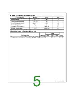
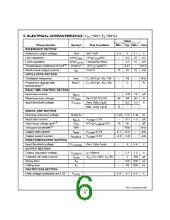
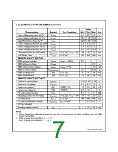
5. ELECTRICAL CHARACTERISTICS
(V =20V, T =25°C)
CC
A
Value
Characteristic
REFERENCE SECTION
Reference output voltage
Line regulation
Symbol
Test Condition
Min. Typ. Max. Unit
Vref
Iref=1mA
4.9
–
5
5.1
25
15
–
V
∆
Vref.LINE 14V<VCC<30V
2.0
1.0
0.01
35
mV
∆
Load regulation
Vref.LOAD 1mA<Iref<10mA
–
mV
Temperature coefficient of Vref(1)
Short-circuit output current
OSCILLATOR SECTION
Oscillation frequency
Vref/ T
-25°C<Ta<85°C
Vref=0
–
%/°C
mA
∆
∆
ISC
15
75
fosc
CT=0.01µF, RT=12k
CT=0.01µF, RT=12k
–
–
10
2
–
–
kHz
%
Frequency change with
temperature(1)
fosc/T
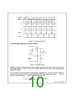
DEAD TIME CONTROL SECTION
Input bias current
IB(DT)
–
45
–
-2.0 -10
µA
%
V
Maximum duty voltage
Input threshold voltage
DCMAX
VTH(DT)
Pin19 (DTC)=0V
Zero Duty Cycle
Max. Duty Cycle
48
3.0
–
50
3.3
–
0
ERROR AMP SECTION
Inverting reference voltage
Input bias current
Open-loop voltage gain(1)
Unit-gain bandwidth(1)
Output sink current
Vref(EA)
IB(EA)
GVO
1.20 1.25 1.30
%
VCOMP=2.5V
–
70
–
-0.1 -1.0 µA
0.5V<VCOMP<3.5V
95
650
0.9
–
–
–
–
dB
kHz
mA
mA
BW
ISINK
VCOMP=0.7V
VCOMP=3.5V
0.3
Output source current
PWM COMPARATOR SECTION
Input threshold voltage
OUTPUT SECTION
ISOURCE
-2.0 -4.0
VTH(PWM) Zero Duty Cycle
–
4
4.5
V
V
Output saturation voltage
Collector off-state current
Rising time
VCE(SAT)
IC(off)
TR
IC=200mA
–
–
–
–
1.1 1.3
VCC=VC=30V, VE=0V
2
100 µA
100 200
50 200
ns
ns
Falling time
TF
PROTECTION SECTION
Over voltage protection for 3.3V
VOVP1
3.8
4.1 4.3
V
Rev C, November 1999
6

 FAIRCHILD [ FAIRCHILD SEMICONDUCTOR ]