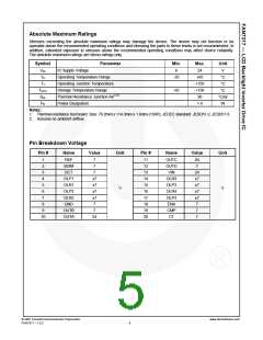
Absolute Maximum Ratings
Stresses exceeding the absolute maximum ratings may damage the device. The device may not function or be
operable above the recommended operating conditions and stressing the parts to these levels is not recommended. In
addition, extended exposure to stresses above the recommended operating conditions may affect device reliability.
The absolute maximum ratings are stress ratings only.
Symbol
VIN
Parameter
Min.
6
Max.
24
Unit
V
IC Supply Voltage
TA
Operating Temperature Range
Operating Junction Temperature
Storage Temperature Range
Thermal Resistance Junction-Air(1,2)
Power Dissipation
-25
+85
+150
+150
90
°C
TJ
°C
TSTG
θJA
-65
°C
°C/W
W
PD
1.4
Notes:
1. Thermal resistance test board. Size: 76.2mm x 114.3mm x 1.6mm (1S0P); JEDEC standard: JESD51-2, JESD51-3.
2. Assume no ambient airflow.
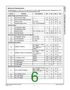
Pin Breakdown Voltage
Pin #
Name
REF
Value
7
Unit
Pin #
11
Name
OUTC
OUTD
VIN
Value
24
7
Unit
1
2
BDIM
BCT
7
12
3
7
13
24
±7
±7
±7
±7
7
4
OLP1
OLR1
OLP2
OLR2
GND
±7
±7
±7
±7
7
14
OLR3
OLP3
OLR4
OLP4
ENA
5
15
V
V
6
16
7
17
8
18
9
OUTB
OUTA
7
19
CMP
CT
7
10
24
20
7
© 2007 Fairchild Semiconductor Corporation
FAN7317 • 1.0.2
www.fairchildsemi.com
5

 FAIRCHILD [ FAIRCHILD SEMICONDUCTOR ]