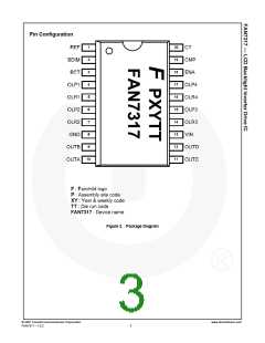
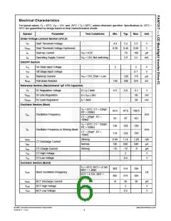
Pin Definitions
Pin #
Name
Description
This pin is 5V reference output. Typically, resistors are connected to this pin from CT pin
and BCT pin.
1
REF
This pin is the input for burst dimming. The voltage range of 0.5 to 2V at this pin controls
burst mode duty cycle from 0% to 100%.
2
3
BDIM
BCT
This pin is for programming the frequency of the burst dimming. Typically, a capacitor is
connected to this pin from ground and a resistor is connected to this pin from the REF pin.
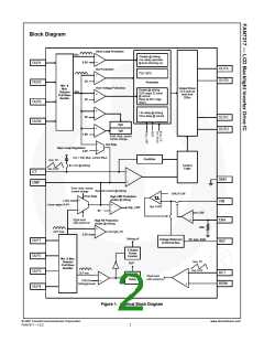
This pin is for open-lamp protection and feedback control of lamp currents. It has the same
functions as other OLP pins and is connected to the full-wave rectifier internally. In striking
mode, if the minimum of rectified OLP inputs is less than 1V for 1.6s; or in normal mode, if
the minimum of rectified OLP inputs is less than 0.5V for 10ms; the IC shuts down to protect
the system in open lamp condition. The maximum of rectified OLP inputs is inputted to the
negative of the error amplifier for feedback control of lamp current.
4
OLP1
This pin is for open-lamp regulation. It has the same functions as other OLR pins and is
connected to the full-wave rectifier internally. When the maximum of rectified OLR inputs is
between 1.8V and 2V, the error amplifier output current is limited to 1µA; and when the
maximum of rectified OLR inputs reaches 2V, the error amplifier output current is 0A and its
output voltage maintains constant. The maximum of rectified OLR inputs is inputted to the
negative of another error amplifier for feedback control of lamp voltage. When the maximum
of rectified OLR inputs is more than 2.2V, another error amplifier for OLR is operating and
lamp voltage is regulated.
5
6
OLR1
OLP2
This pin is for open-lamp protection and feedback control of lamp currents. Its functions are
the same as the OLP1 pin.
7
OLR2
GND
This pin is for open-lamp regulation. Its functions are the same as the OLR1 pin.
This pin is the ground.
8
9
OUTB
OUTA
OUTC
OUTD
VIN
This pin is NMOS gate-drive output.
10
11
12
13
14
This pin is PMOS gate-drive output.
This pin is PMOS gate-drive output.
This pin is NMOS gate-drive output.
This pin is the supply voltage of the IC.
OLR3
This pin is for open-lamp regulation. Its functions are the same as the OLR1 pin.
This pin is for open-lamp protection and feedback control of lamp currents. Its functions are
the same as the OLP1 pin.
15
16
17
18
19
OLP3
OLR4
OLP4
ENA
This pin is for open-lamp regulation. Its functions are the same as the OLR1 pin.
This pin is for open-lamp protection and feedback control of lamp currents. Its functions are
the same as the OLP1 pin.
This pin is for turning on/off the IC.
Error amplifier output. Typically, a compensation capacitor is connected to this pin from the
ground.
CMP
This pin is for programming the switching frequency. Typically, a capacitor is connected to
this pin from ground and a resistor is connected to this pin from the REF pin.
20
CT
© 2007 Fairchild Semiconductor Corporation
FAN7317 • 1.0.2
www.fairchildsemi.com
4

 FAIRCHILD [ FAIRCHILD SEMICONDUCTOR ]