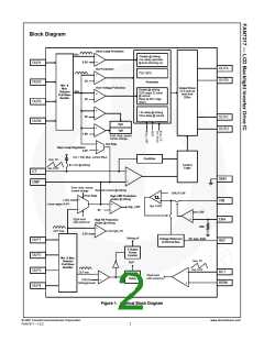
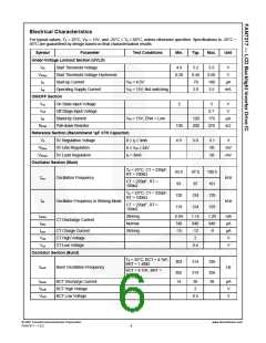
Block Diagram
Short Lamp Protection
Min.
-
Disable @ striking
1ms delay (operation
@ burst dimming on)
0.3V
+
OLR1
OLR2
OUTA
OUTB
Arc Protection
TSD 150oC
+
-
3V
2V
Protection
Min. &
Max.
Detector
/Full Wave
Recifier
Over-Voltage Protection
Output Driver
7V 0.2A/0.3A
dead time
Disable @ striking
OLR output 32 count
@ normal
Reset by BCT edge
detect
Max.
+
-
200ns
OLR3
OLR4
+
1.6s delay @ striking
10ms delay @ normal
2V
OUTC
OUTD
-
0μA
+
1μA
1.8V
-
Error. Amp. source
current change
Gm Amp.
-
Open Lamp Regulation
2.2V
+
Gm = 350, Max. current 85μA
Oscillator
max. 2V
Control
Logic
On @ striking
min. 0.5V
CT
-
GND
+
CMP
Error. Amp. source
current change
0μA sink current @ striking
-
UVLO 5.5V
Error Amp.
High CMP Protection
disable @ striking
1.35V
Linear region 0~4V
+
-
+
VIN
+
Hys. 0.45V
High_CMP
3V
-
-
1.35V
+
52μA burst
sink current on
ENA
High FB Protection
disable @ striking
200k
+
OLP max.
High_FB
3.5V
-
Striking off
Voltage Reference
& Internal Bias
5V, max. 3mA
OLP1
OLP2
OLP3
OLP4
REF
4 Output
Pulses
Counter
Min. & Max.
max. 2V
Detector
/Full Wave
Rectifier
OLP
min. 0.5V
-
BCT
OLP min.
-
150μs
Delay
52μA burst
sink current on
1V/0.5V
Striking/normal
+
+
BDIM
Figure 1. Internal Block Diagram
© 2007 Fairchild Semiconductor Corporation
FAN7317 • 1.0.2
www.fairchildsemi.com
2

 FAIRCHILD [ FAIRCHILD SEMICONDUCTOR ]